
Are yo wondering what is the PLCC package? Trying to understand this crucial component, but actually, it’s quite hard to bring out clear information. You are not alone. Many people find it difficult to figure out electronic packaging and most importantly—PLCCs.
Don’t worry; that’s what this article is here for. We will explain everything you need to know about PLCC packages in simple terms.
So let’s get started.
What is the PLCC Package
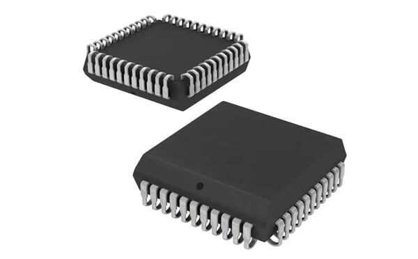
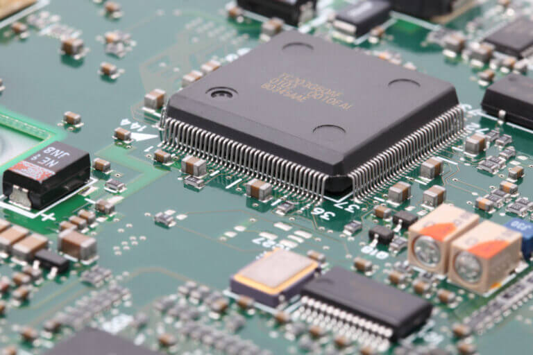
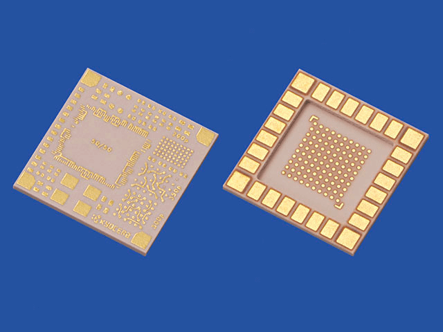
PLCC stands for Plastic Leaded Chip Carrier, which is a type of surface-mounted integrated circuit package. The shape is mostly rectangular or square, with a lead or pin that extends from one side of the package shaped in a “J” form.
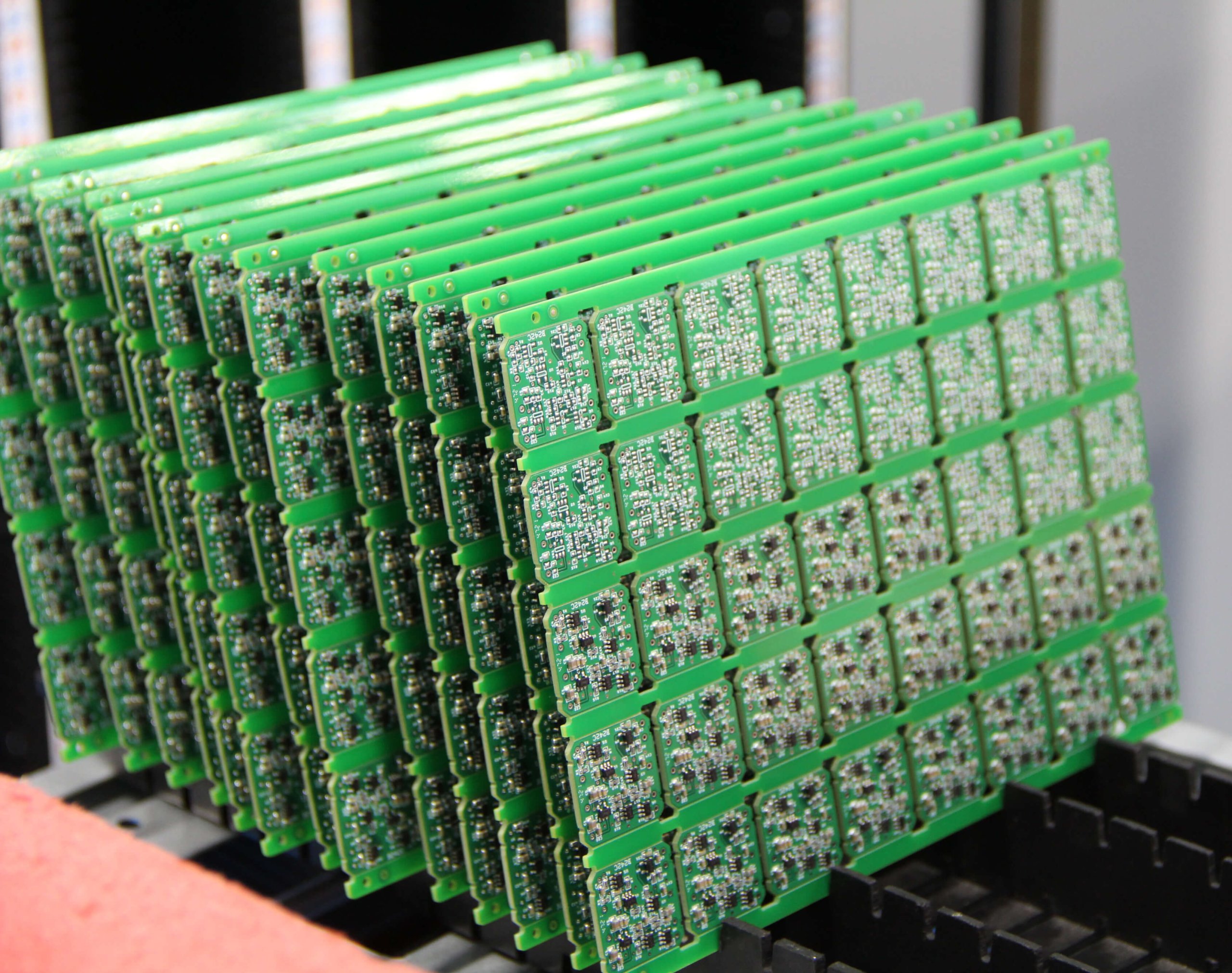
They offer PLCC a kind of leads that allow direct soldering into a Printed Circuit Board (PCB). Broad applications find place with PLCC packages in every kind of electronics equipment just because of the two reasons that characterize them- ruggedness and space.
PLCC Package Structure
The PLCC package consists of several key physical components that contribute to its functionality and durability:
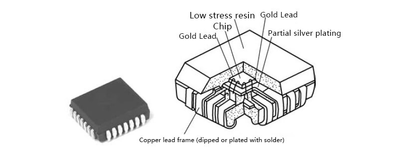
- Body: A PLCC package mainly involves a higher temperature plastic and thus forms the main body structure, which provides a good force spillover for safe and stable support to the internal integrated chip.
- Leads: These are in the shape of a “J” and extend from the package, allowing the PLCC to be soldered onto the board in a very secure manner. These leads are in contact with the IC and electrically connected to the board thoroughly.
- Pins: In PLCC packages, the number of pins may be between 20 and 84; these provide various connection points for an IC.
Dimensions and Standards
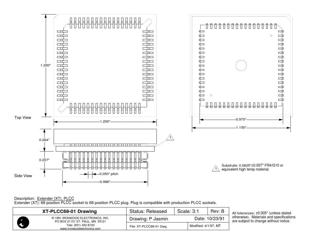
PLCC packages are designed following international standards to ensure PCB and component compatibility. The standards are determined by the JEDEC.
The standard dimensions and variations include:
- Body Size: The package body size can range from 9 mm x 9 mm all the way to 27 mm x 27 mm, based on the size and function of the IC.
- Pin Counts: The flex cable has 20 to 84 pin counts, making it quite flexible for use in various applications in many fields.
Comparison of Different PLCC Package Types
PLCC packages come in several types, each designed for specific applications and requirements:
- Standard PLCC: This is the most used variety of PLCC, suitable for very many general-purpose electronic applications.
- Thin PLCC (T-PLCC): Thin PLCC, developed with a lowered profile for low profile applications in space-constricted modules.
- Quad Flat Package (QFP): One of many variations of the standard PLCC, the QFP has leads extending under all four sides around the entire package. This allows for different methods of mounting and connections.
A strong body and secure, trusted leads are the features of the PLCC package, along with different pin configurations, which can extensively be fit in many electronic applications.
Furthermore, its adherence to industry standards ensures it can be used seamlessly in a variety of designs and environments.
Materials Used in PLCC Packages
PLCC packages are made of materials that are resistant to damage, effective in terms of electrical characteristics, and able to endure the widest range of environmental hazards.
- Body: The outline of a PLCC package is normally fabricated using a high-temperature plastic. The material is chosen to seal the internal integrated circuit from any form of physical damage, moisture, and other environmental factors. The plastic used is also resistant to high temperatures, thereby making them suitable during soldering and in the entire life of the device’s operation.
- Leads: The electrical contacts in a PLCC package are mostly made from copper alloy. Very high electrical conductivity in copper guarantees a good interaction signal between the IC and the PCB. The leads are also given mechanical robustness by the use of copper alloys, allowing them to withstand handling during assembly and thermal cycling stresses.
Material Properties and Their Impact on Package Performance
The selection of materials for PLCC packages has major effects on performances and reliabilities in electronic applications.
- Plastic Body: Some clear advantages of high-temperature plastic material for PLCC bodies are pointed out. Its mechanical protections and septa make a strong enclosure for the IC and protect it from mechanical damage and some minor environmental harm. The high-temperature resistance of plastic makes sure that the package processes of soldering leave the survivors without deformation so that the integrity of the circuit inside is not impaired.
- Lead Copper Alloys: Copper alloys used for leads provide great electrical performance with efficient signal transmission and a low resistance level. Besides the high mechanical strength in copper alloys, the metallurgical characteristic also helps in holding the integrity of leads while handling, during the soldering process, and while in operation. It helps with the required kind of reliable operation for long-term functioning rather than frequent connection failures.
PLCC Package Applications
PLCC packages find large acceptance because of all these several applications as an essential part of many varieties of electronic gadgets, and for their reliability. They are eminently used in home appliances, industrial machines, consumer electronics, computer systems, etc
- Microcontrollers: PLCC packages are ideal for the packaging of microcontrollers for key components in embedded systems, consumer electronics, automotive controls, and industrial automation.
- Memory Chips: Many memory chips, such as ROMs and RAMs, use PLCC packages due to their compact size and ease of integration into various PCB layouts.
- Integrated Circuits (ICs): PLCCs are utilized with a broad range of IC devices including logic chips, analog circuitry, and custom ASICS because of their rugged construction and the provision of a reliable connection.
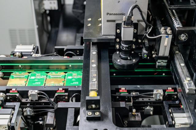
PCB Design Considerations for PLCC Packages
Here are some PCB design considerations for PLCC packages that will help you:
1)Land Pattern Design Specifics for PLCC Packages
Land pattern design for PLCC packages is thoroughly important for the right formation of solder and reliable connections. Among the many important considerations are:
- Pad Size and Spacing: Pad size and spacing must be compatible with the leads. This ensures that perfect alignment is made between these and the pads on the PCB during soldering.
- Solder Mask: A solder mask shall be applied between pads so that bridging of solder between leads is prevented. The solder mask helps to define the solderable areas, and its application enhances the reliability of the solder joints overall.
- Standoff Height: The land pattern shall incorporate an allowance of the standoff height of the PLCC package to ensure there is room for solder flow and the correct co-planarity of the component.
2)Thermal Management Strategies for PLCC Packages
Good thermal management plays a key role in making sure that the PLCC packages become effective and reliable in various high-power applications.
- Thermal Vias: Thermal vias are yet another method to dissipate the heat away from the PLCC package through the incorporation of them into the PCB design. These are actually the vias that connect the top layer with an inside or bottom layer of a PCB which creates a path of flow for the increase of temperatures to dissipate away.
- Heat Sinks: The addition of heat sinks to the PCB or to the PLCC package itself seriously enhances thermal management. Heat sinks attach additional surfaces for heat dissipation, therefore the assembly maintains its component temperatures at relatively safe levels.
- Copper Pour: Copper poured in the PCB, encircling the PLCC, increases the area in doing so and hence proves beneficial for heat dissipation. The copper pour works like a heat spreader, which simply spreads the heat generated by the segment to a wider area.
3)Component Placement and Routing Guidelines
Thus, performance and reliability optimization for PLCC packages will highly be dependent upon the proper placement/routing of its components.
- Component Spacing: Avoid signal loops between the PLCC package and other components on the PCB; it allows some distance, which helps in managing the heat wave and reduces the hazards of causing noise events or short circuits.
- Signal Integrity: High-speed signal traces should be routed very carefully to avoid noise and signal degradation. Avoid routing sensitive traces close to power lines or any other noisy areas of the PCB.
- Power and Ground Planes: Power and ground planes should be separate to eliminate power distribution problems and/or drive Electric and Magnetic Radiation. Pay careful attention if the PLCC packages contain any high-speed or sensitive circuits.
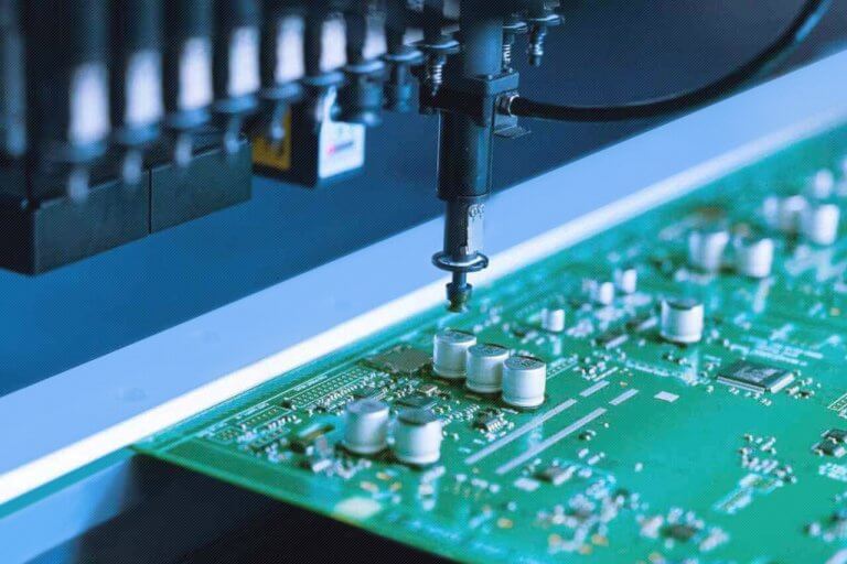
4)Soldering Techniques Suitable for PLCC Packages
Reliable solder joints for the PLCC packages are needed, along with the correct technique of soldering.
- Reflow Soldering: The majority of PLCC packages require this technique in the assembly. In this procedure, a solder paste is placed on the pads located on a PCB, and the respective components are mounted. The product is later passed through a reflow oven whereby the solder melts and performs important joining processes.
- Wave Soldering: Wave soldering is relatively less popular for the PLCC package but still applicable in certain PLCC scenarios. All the plated metal areas are passed over a wave of molten solder, which selectively solders to the exposed metal surfaces and forms solder joints. This process is quite suitable for through-hole component soldering, from which PLCC packages can borrow proper design consideration.
- Hand Soldering: Hand soldering can be done where small-scale production or repair work is required. However, a fine-tip soldering iron should be used with good temperature control. Care should be taken to prevent the overheating of components and to ensure even distribution of the solder.
Conclusion
Understanding what is the PLCC package is crucial for anyone involved in electronics. PLCC packages are essential components in many devices due to their compact size, durability, and reliable performance. They are used in microcontrollers, memory chips, and various integrated circuits.