


Do you find it difficult to achieve signal integrity in your PCB design? You are not alone. The majority number of designers face this problem, yet maintaining signal integrity is quite important for reliable passing of data in most modern electronic devices.
The complexities of high-speed signals, impedance mismatches, and noise interference can make achieving signal integrity feel like a daunting task.
Don’t worry, though. This article will go with you every step of the way in terms of what you need to know concerning signal integrity in the printed circuit board design process.
So, by the end of this article, you will have both the means and confidence to deal with signal integrity problems and optimize your PCB layout for peak performance.
What is Signal Integrity in PCB Design
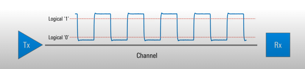
Signal integrity in PCB design is the capability of the PCB to transfer any electrical signal from a source to a receiver without distortion or degradation along the path.
Think of this as a way to ensure that your signal’s path through your circuit board is as faithful as the syllabus is to the information. So, to sum up, signals have good integrity when they get to the other end as they should, with no changes that were not intended.
Of course, this is very important for the proper functioning of electronic devices, especially today, when the speed of data transmission is growing very fast; even the least impairment of the signal could cause huge performance issues.
Now let’s discuss the importance of signal integrity in PCB designs in detail.
Importance of Signal Integrity in PCB Designs
As said earlier, signal integrity is a principal dimension of PCB design affecting the proper functioning of electronic devices. Other than that, there are a few reasons why it is so essential.
Let’s review them in more detail.
Reliable Data Transmission
In the high-speed electronic device era, good signal integrity is important for data transmission accuracy and reliability. In digital systems, signals are used to transfer binary data among various components.
Whenever there is any distortion, attenuation, or noise in the signal, it is likely to cause some kind of error in data interpretation at the receiver.
By ensuring good signal integrity, the designer assures the proper reception of the transmitted signals, thus reducing the possibilities of data errors and ensuring communication integrity.
Reduced Errors
Good signal integrity helps in preventing bit errors or glitches, which could be included in the data while transmitting.
Disturbances that are relatively small, potentially caused by reflections, crosstalk, or impedance mismatches in the signal path, can be made into errors or glitches and may propagate in the system and cause failure.
By adopting good signal integrity practices in the PCB design stage, such as controlled impedance routing, signal termination, and reduction of electromagnetic interference, the designer can minimize the error probability and, hence, improve overall system reliability.
Functional Circuits
The printed circuit board will work problem-free, like no corrupted data or system crash, as long as signal integrity is retained. Most often, in the more complex electronic systems, a host of different signals will cross the PCB, carrying important information in transit between the components.
Any form of signal degradation can turn out to interfere with the circuit’s operation and lead to operational failures or performance degradation.
Thus, the highest design priority of signal integrity has been given to overcome signal degradation risks and to let the electronic system work properly under a variety of working conditions.
Thus, emphasizing signal integrity in your design will be enabling the best performance and reliability to be designed into your PCBs.
Now, let’s discuss some factors that might deteriorate signal integrity in your PCB design.
Factors Degrading Signal Integrity in PCB Designs
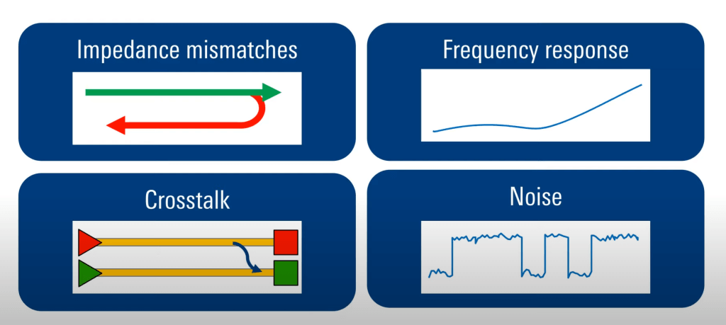
As you know, achieving and maintaining signal integrity in PCB designs can be a complex task, often challenged by various factors that can degrade the quality of electrical signals.
Let us describe these factors one by one:
1.Signal Loss
Since the signals are basically waves in this case, they will undergo a certain amount of resistance during the process of propagation over PCB traces. This happens especially with high-frequency circuits.
The increased trace width, thickness, and material properties enhance the resistance of the trace, which leads to attenuation or loss of a signal. There may even be increased losses due to such phenomena as skin effect, where high-frequency signals have a tendency to propagate along the surface of conductors.
2.Reflections
An impedance mismatch at the end of the transmission line causes part of the signal to be reflected back to the source. These reflections combine with the main signal and create signal distortion, which may eventually lead to data errors.
Trace width variations, vias, connectors, and transmission-line discontinuities are the most common sources of impedance mismatch.
3.Crosstalk
In high-density PCB layouts, there could be coupled electromagnetics between the adjacent traces, leading to the formation of crosstalk. This causes unwanted signals generated on one trace to interfere with the others, thus distorting signal integrity.
Crosstalk deteriorates with higher frequencies and can be taken care of by proper trace spacing, shielding, and proper signal-routing techniques.
4.Noise
Various types of noise, such as external electromagnetic interference, power supply noise, and ground bounce, can be introduced into the signal path, therefore degrading signal integrity.
Noise normally appears in the form of unwanted voltage fluctuations superimposed on the signal, distorting the clarity and reliability of the signal. One has to consider shielding sensitive traces, low-noise power supplies, and proper grounding techniques in order to prevent signal degradation by noise.
By understanding and addressing these factors, PCB designers can implement strategies to preserve signal integrity and ensure optimal performance of their designs.
But what are the strategies? Don’t worry, let’s discuss them below.
Techniques to Maintain Signal Integrity
There are different techniques to overcome challenges and maintain signal integrity in your PCB designs.
Here are some important ones that you must know:
- Controlled Impedance Routing
Impedance control has a great deal to do with the idea of uniformity. Strict control over the impedance of signal traces within the layout can serve as a great way to reduce signal reflection as well as impedance mismatches.
This involves adhering to certain trace widths, spacing, and layer stack-up configurations to strike the specified impedance. That is particularly the case for high-speed signals.
- Proper Termination Techniques
Termination plays a crucial role in preventing signal reflections at the receiving end of a trace. An ideal termination in series or parallel to the ground will absorb any reflected signal and then maintain a better signal integrity.
Matching the termination impedance to the characteristic impedance of the transmission line will considerably minimize signal distortion for good signal integrity.
- Minimizing Trace Length
Long traces act like antennas and are always prone to signal loss and electromagnetic interference. The purpose of having traces at a short length is to reduce the signal propagation delay while keeping the impact of attenuation on the signal propagation at a minimum.
This can be achieved by carefully placing the components and optimizing the route to ensure that the more critical high-speed signals have the minimum possible trace length with respect to signal integrity.
- Grounding and Shielding
Ground planes and shielding are two powerful tools the PCB designer has to reduce noise and crosstalk. Large ground planes reduce overall impedance in the return path for a signal, effectively reducing ground bounce and electromagnetic radiation.
Proper shielding that creates a barrier between sensitive areas or signal routing ensures that electromagnetic emissions stay where they are supposed to and interference from the outside does not corrupt signal integrity.
- Impedance Matching for Differential Pairs
Differential signaling is commonly applied for the high-speed transmission of data, as it has immunity to common-mode noise. Impedance matching between the two traces of a differential pair is very important from a signal integrity viewpoint.
Maintaining consistent trace widths, spacing, and characteristic impedance along the length of the pair minimizes signal reflections and hence maximizes the integrity of the signal.
The differential pair routing rules consider parameters like controlled differential impedance and length matching, which should be taken into consideration in order to optimize the quality of signal and minimize the effects of electromagnetic interference.
Whether working on high-speed digital circuits or sensitive analog systems, signal integrity is key to reliable, repeatable operation. And these techniques will help you at every step.
Conclusion
In conclusion, signal integrity is one of the important topics in PCB design, ensuring that data transmission is reliable and the electronic device performance is fully optimized.
After comprehending the significance of signal integrity, ways of detecting SI degradation, and the application of effective techniques for its maintenance, the designer will make it through the challenge of delivering a great PCB design.