Have you ever thought about how your electronic device can work perfectly with all of those complicated circuits inside? The magic happens with routing which is an integral step in PCB design. But everything that has to deal with routing seems pretty complicated, especially for beginners.
However don’t worry, because this article is here to enlighten you on everything to do with routing in PCB design. From what is routing in PCB design, different routing techniques, to effective routing tips, we will discuss everything to help you.
So let’s get started.
What is Routing in PCB Design
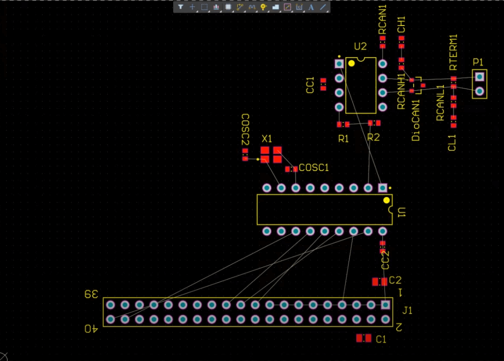
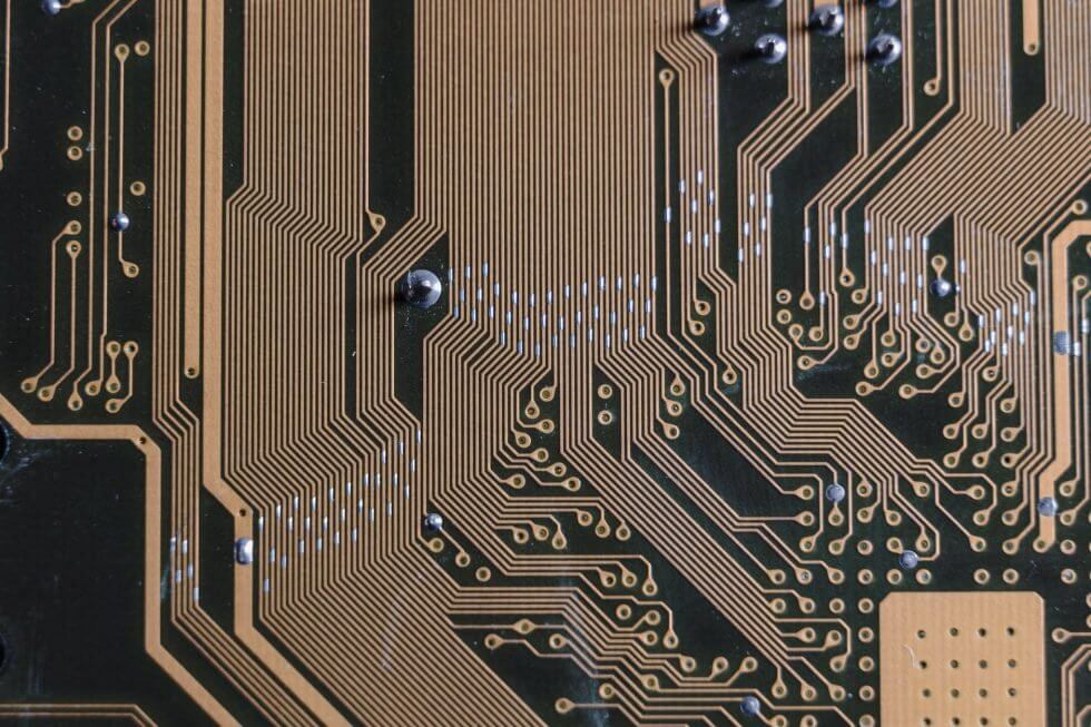
Well, routing in PCB design is the process of planning and creating the electrical connections between components on a printed circuit board using conductive traces etched onto the board’s surface.
These traces act to provide a conduction path for electrical signals to interconnect active devices, such as integrated circuits, resistors, capacitors, and connectors, inside a device to be able to function as a working circuit.
The goal of routing is to come up with efficient and reliable connections at the same time, meeting design constraints such as signal integrity or constraints in relation to electromagnetic compatibility and considerations on manufacturability.
Routing is done in such a way that it ensures the best performance and functionality for the electronic devices.
There are differnet types of routing techniques used in PCB design that you must know. Let’s discuss them in detail.
Different Routing Techniques in PCB Design
As said above, PCB routing defines the efficiency and performance of electronic circuits to a large extent.
So here are the different routing techniques that you must know:
1.Point-to-Point Routing
The idea behind this technique is to connect the PCB components by the direct path with the smallest trace lengths. The primary objective is to minimize the signal propagation delay, signal distortion, and interference of electromagnetic signals.
Reducing the length of traces can cut down the signal loss and maintain the best possible integrity of a signal. These are more critical in high-speed designs, where even small delays can result in considerable performance loss.
Point-to-point routing is usually implemented in high-performance signal timing-sensitive applications, such as critical high-frequency circuits and systems.
While this may be effective in reducing signal path lengths, it may be done at the expense of giving a more complicated and filled-up layout that may need proper planning and optimization to give out the desired performance output.
2.Grid Routing
Grid routing is the definition of the alignment of traces and components to the grid system, generating some kind of organized and predictable routing pattern in the PCB.
Staying on grid allows for maintaining equal trace spacing while hitting the board’s constraints, such as minimum trace width and clearances.
Grid-based routing can simplify the process of routing in a structured way for the placement of traces, characterized by its achievements in achieving a clean and tidy layout.
This in turn allows an efficient use of real estate for PCB fabrication, better manufacturability, and lower error probabilities for routing and design rule violations.
Even though grid routing supports many features that can be helpful to attain a consistent layout and manufacturability, it is not always desirable for a design featuring irregular component placement or complex routing requirements.
3.Differential Pair Routing
Differential pair routing is a specialized technique used for high-speed signals, particularly in differential signaling applications like USB, HDMI, and Ethernet interfaces. It involves routing two closely spaced traces on the PCB, carrying equal and opposite polarity signals.
The close proximity of the traces helps to minimize electromagnetic interference and crosstalk, ensuring robust signal integrity and reducing the susceptibility to external noise sources. Proper impedance matching and controlled trace geometry are crucial aspects of differential pair routing to maintain signal quality and prevent signal degradation.
Designers must also consider factors such as skew, length matching, and routing symmetry to ensure accurate signal transmission and reception.
Differential pair routing is essential for achieving reliable communication and data transmission in high-speed designs, where signal integrity is paramount.
4.Bus Routing
Bus routing involves grouping signals together and routing them along shared pathways called buses. This technique simplifies layout and reduces congestion by consolidating multiple signals into a single routing channel.
By minimizing the number of individual traces, bus routing can streamline the PCB design process and improve overall design efficiency. It is commonly used in applications with multiple interconnected components or subsystems, such as microprocessors, memory modules, and peripheral interfaces.
Bus routing helps to optimize signal routing and minimize signal propagation delays, enhancing the performance and reliability of the overall system.
However, designers must carefully manage signal assignments and consider factors such as signal loading, impedance matching, and signal integrity to ensure proper bus operation and prevent signal degradation.

Effective Routing Tips for PCB Design
Now you know the basics of routing in PCB design, it’s time to discuss some effective routing tips for PCB design.
Here they are:
- Minimizing Trace Length
Keeping trace lengths as short as possible is crucial for optimizing signal integrity, particularly in high-speed designs. Longer traces increase signal propagation delay and susceptibility to external noise, leading to signal degradation and performance issues.
By minimizing trace lengths, designers can reduce signal loss, improve signal integrity, and ensure reliable signal transmission throughout the PCB.
Techniques such as careful component placement, direct routing paths, and signal optimization can help achieve shorter trace lengths and enhance overall design efficiency.
- Maximizing Clearance
Proper clearance between traces is essential for preventing electrical shorts and minimizing crosstalk between adjacent signals. Insufficient clearance can result in signal interference and signal integrity issues, compromising the performance of the PCB.
Designers should adhere to design rules and specifications to maintain adequate clearance between traces, ensuring reliable operation and minimizing the risk of electrical failures.
Techniques such as design rule checks (DRC) and clearance optimization tools can help identify and resolve clearance violations, ensuring compliance with industry standards and best practices.
- Avoiding Sharp Bends
Sharp bends in traces can introduce unwanted signal reflections and impedance mismatches, degrading signal quality and causing signal integrity issues. It’s essential to minimize sharp bends and maintain smooth routing paths to ensure optimal signal transmission and reception.
By avoiding sharp corners and utilizing gradual bends or curves, designers can reduce signal distortion and improve the overall performance of the PCB.
Techniques such as utilizing curved trace segments, optimizing routing paths, and employing interactive routing tools can help achieve smoother trace routing and enhance signal integrity.
- Multilayer PCB Utilization
Multilayer PCBs offer numerous benefits for complex designs, including better routing organization and signal isolation with internal layers. By distributing signal layers across multiple PCB layers, designers can optimize routing density, minimize signal crosstalk, and enhance overall design flexibility.
Multilayer PCBs also enable the integration of power and ground planes, providing a stable reference for signal routing and improving signal integrity. Designers should leverage multilayer PCB technology to optimize signal routing, minimize electromagnetic interference, and achieve optimal performance in high-density and high-speed designs.
Techniques such as layer stackup planning, signal layer allocation, and via optimization can help maximize the benefits of multilayer PCB utilization and ensure successful design implementation.

Additional Design Considerations Influencing Routing Decisions
By knowing different routing techniques for PCB design, you must be wondering how to further optimize your designs for maximum efficiency and performance. Additional design considerations play a crucial role in influencing routing decisions and ensuring the success of your PCB layouts.
Let’s discuss them in detail.
Component Placement:
Strategic component placement is essential for minimizing trace lengths, reducing signal interference, and improving routing efficiency. By carefully positioning components on the PCB, designers can optimize signal paths, streamline routing, and enhance overall design integrity.
Close proximity between related components, such as microcontrollers and associated peripherals, can help minimize signal propagation delays and improve signal quality.
Additionally, grouping components with similar functions can simplify routing and minimize the risk of signal crosstalk, ensuring reliable operation of the PCB.
Power and Ground Planes:
Power and ground planes play a crucial role in providing stable voltage references, reducing noise, and improving signal integrity. By integrating power and ground planes into the PCB layout, designers can minimize voltage fluctuations, mitigate electromagnetic interference, and enhance overall signal quality.
Proper placement and distribution of power and ground connections are essential for ensuring uniform voltage distribution and minimizing signal noise.
Designers should pay attention to power plane capacitance and impedance matching to optimize power delivery and maintain signal integrity throughout the PCB.
Design Rules Check (DRC):
Design rule checks are essential for identifying and correcting potential routing errors, ensuring compliance with design specifications and industry standards. By performing DRC checks using PCB design software, designers can detect issues such as insufficient clearance, excessive trace lengths, and signal integrity violations.
Addressing these issues early in the design process helps minimize the risk of electrical failures, improve design reliability, and streamline manufacturing. Designers should regularly perform DRC checks throughout the design process to identify and rectify potential routing errors, ensuring the successful implementation of their PCB layouts.
By considering these additional design considerations, you can further optimize their routing decisions and ensure the successful realization of their PCB designs.
Conclusion
In conclusion, mastering routing in PCB design is crucial for creating efficient electronic devices. Understanding techniques discussed above, you will be able to optimize signal paths and minimizes interference.
Moreover, considering additional factors like component placement, power and ground planes, and design rule checks further ensures successful layouts.


