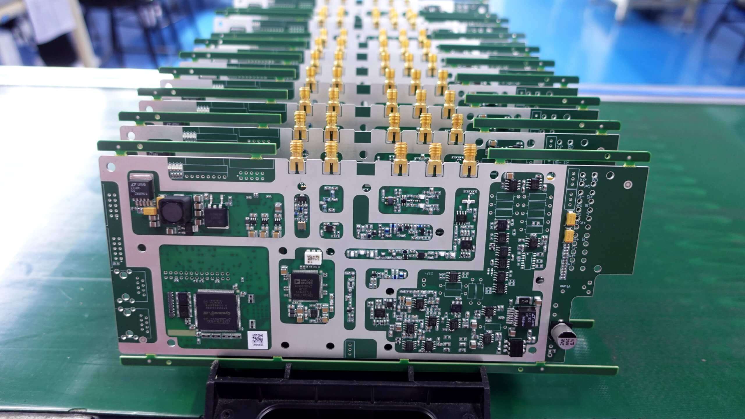
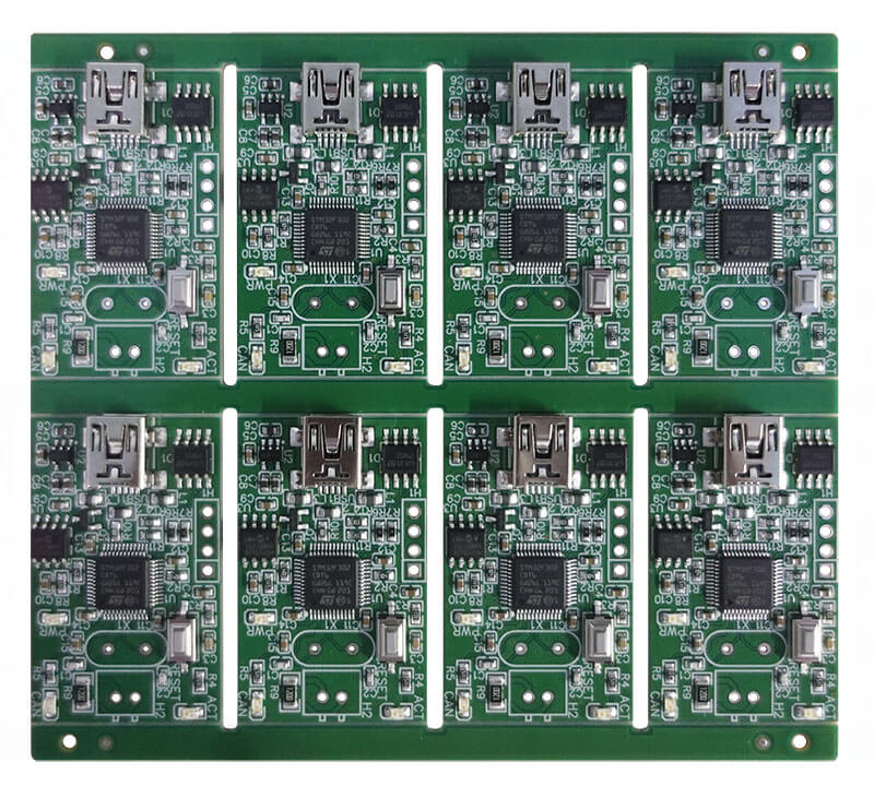
Ever wonder how your smartphone or computer works? A Printed Circuit Board (PCB) is the heart of all these devices. It is the backbone of modern electronics. All electronic components are placed and interconnected on it.
So, how do these boards come alive? PCB assembly handles this by electrically connecting electronic components on top of the PCB. It ensures that each part works properly and communicates with each other.
You must be wondering why PCB assembly is so important. Without it, we wouldn’t have the working phones and computers we depend on so much in our daily lives. PCB assembly turns a simple board into a powerful complex unit.
Today, we will discuss PCB assembly. We will explain how this works, the technologies used, and why it is important. So, let’s get started!
What is Printed Circuit Board Assembly (PCBA)
Printed Circuit Board Assembly (PCBA) is the entire process of mounting components on a blank PCB board through SMT equipment or inserting components through DIP.
Now that we understand the basic definition of PCB assembly, it’s time to explore the technologies used in circuit board assembly. Each technology has advantages and is suitable for different applications. Let’s look at how these technologies and how they come together to create the devices we love.
Types Of PCB Assembly Technologies
●Surface Mount Technology (SMT)
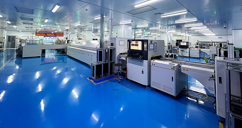
One of the most common methods of assembling a PCB is Surface Mount Technology (SMT). In this method, miniature components are placed directly on the surface of the PCB. Solder paste and reflow soldering techniques are used.
Automated pick-and-place machines accurately place the components from reels on the PCB. The board then passes through a reflow oven. While the solder paste melts and holds every part in place when it cools down.
Benefits of SMT:
- Smaller Size: SMT components are small and can lead to compact and lighter designs.
- Higher Density: It allows circuit boards to pack more components onto a single board. It increases functionality without increasing size.
- Faster Assembly:Automatic pick-and-place machines can correctly place components on the PCB. It leads to quicker manufacturing.
●Through-Hole Technology (THT)
This method inserts the components with wire leads passing through drilled holes in a PCB. The leads are soldered on the other side to hold those components in place.
This often requires manual placement of components or auto-insertion machines for high-volume production. After the components are assembled, the board usually undergoes wave soldering. It shuffles over a molten solder well that connects the leads to the PCB.
Benefits of THT:
- Robust for Larger Components: THT is preferred, especially for components. Those that require mechanical robustness, such as connectors and large capacitors.
- Easier Rework: THT components are easy to re-sold or replace. It makes them good for prototypes and low-volume manufacturing practices.
●Mixed Technology Assembly
Mixed-technology assembly uses SMT and THT together into a single PCB. This is needed when printing a project with small, high-density components and large pieces with more mass. First, the SMT components are inserted and soldered. Then, THT components are assembled later. This process combines the power of both to enable Complex and flexible PCB design.
General Steps In PCB Assembly
After exploring the types of PCB assembly technologies, we shall now look at how these technologies are implemented. To keep a PCB fully up and running, following the steps below are to be considered. With this, we simply set and lock all the components right. Let’s discuss it!
1.Solder Paste Stenciling:
The initial phase of PCB assembly is the application of the solder paste to the PCB pads. A stencil (thin, stainless-steel sheet) that has openings in the positions of pads on the PCB is used for this job.
The stencil is laid over the PCB, and the solder paste is spread across it. Once the stencil is removed, the paste will remain on the pads where components should be placed. This paste only temporarily holds the parts together and later forms the solder joints.
2.Pick and Place:
Now, it is time for the PCB to go under the pick-and-place machine. This automated machine consists of accurate robotic arms with vacuum nozzles.
It picks up surface-mount components from reels and places them onto the PCB, where a solder paste is coated. It is a programmed machine that positions each part onto the board at its proper position with precision and time-savings.
3.Reflow Soldering:
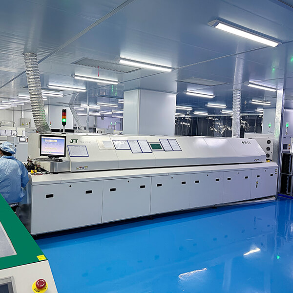
Once the components are placed, the PCBs are reflow soldered. The board is then fed through a reflow oven with various temperature zones.
During the passage through the oven, the solder paste melts and solidifies. It creates permanent solder joints that attach them as components to the PCB. This step ensures that all the components are connected firmly and electrically.
4.Through-Hole Component Assembly (THT Only):
Through-hole components involve inserting the leads of a component through pre-drilled holes on the PCB itself. This can be done manually or with automatic plug insertion machines for larger production runs. After the parts are set, they remain in place for the upcoming soldering phase.
5.Wave Soldering or Selective Soldering (THT Only):
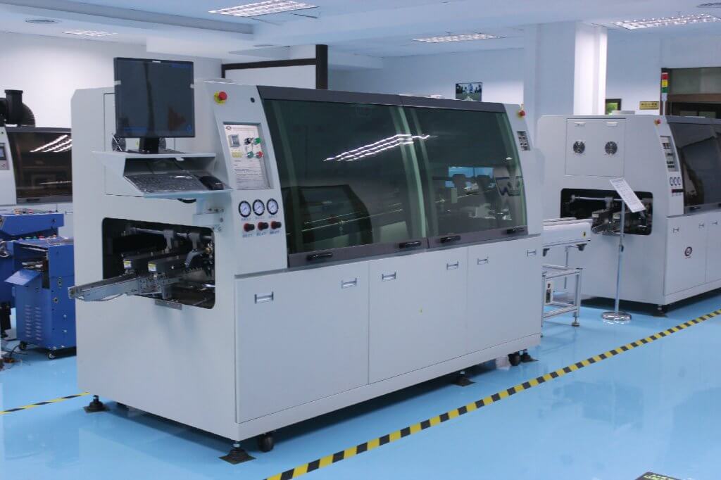
During this phase, PCB with through-hole components move over and is exposed to a wave of molten solder. The hot solder will stick to the exposed metal surfaces. Strong connections are made on both sides of the PCB. Sometimes, we just have to place solder on certain parts. This is where selective soldering steps in. It targets delicate components to avoid heat damage.
6.Inspection and Testing:
The final stage of the assembly process involves checking and testing printed circuit boards. The first step is to perform a visual inspection and verify that the components are correctly placed. Make sure that there are no bad solder joints or missing parts.
Automated optical inspection (AOI) systems make the inspection detailed and fast. Some electrical tests are performed to ensure the PCB is working correctly. These may include functional tests, in-circuit testing (ICT), and sometimes X-ray inspection to identify hidden solder joint problems.
Conclusion
Electronic components are connected to the PCBs through automated and manual methods. Surface Mounting and through holes are essential to understanding how basic boards work. We have discussed the process from the application of solder paste to the final inspection.
You have read about the general steps of PCB assembly to meet a high-end PCB for gadgets. With more advanced techniques, PCB assembly will become high-quality and lower in cost.

