


Are you curious to know how does PCB is manufactured? What is the process? If yes, you are on the right page as here we are going to explain everything about PCB manufacturing.
Being a PCB designer, electronics engineer, or electronics circuit enthusiast, it is important to understand the overall process behind PCB manufacturing. This way, you get an idea of how your design looks when made to life and make better and more efficient PCBs in return.
At the end of this guide, you will have a complete understanding of every single step to carry it through with wisdom in your project.
So, let’s start.
What is PCB Manufacturing?
A printed circuit board or a PCB is an essential part of most modern electronic devices. It provides mechanical support and electrically connects electronic components using conductive strips of copper, also known as tracks or traces, that are etched from laminated copper sheets attached to a non-conductive substrate.
PCBs are present in virtually every electronic device, from simple gadgets such as calculators to very complex systems, including computers and industrial machines.
The manufacturing of PCBs is an intricate process to convert a designed PCB into an actual physical circuit board. It includes several steps: design review, material selection, fabrication, and assembly.
The goal is to create a reliable and high-performance board with exact requirements for its intended application.
The PCB Manufacturing Process
The PCB manufacturing process involves several key stages to transform a PCB design into a functional circuit board.
Let’s explain each stage in detail:
1.Design Review and File Preparation
First of all, the DFM of the design should be verified. This means looking throughout the design files for mistakes, ensuring that they meet manufacturing capabilities, with an optimized layout in a way that could avoid potential production issues.
After the first design is confirmed, production files are generated. Sometimes called Gerber files, these are the files that contain everything needed for manufacturing: layer structures, drill patterns, and component placements.
2.Material Selection
Appropriate base materials are selected based on the design requirements. Suitable base materials include FR4, which is used in about 90% of the boards. It is a composite of epoxy resin and glass fiber, known for its toughness and insulating propensities.
The conductive layers are, therefore, implemented using electrical pathways, generally in the form of thin copper layers. In exceptional cases, materials such as Rogers are utilized for their high electrical performance features.
3.Panel Fabrication
Large panels with repeat PCBs are created using a photolithography and etching technique. Photolithography is adding a photo-resist mask of the PCB onto the panel and then using UV light on it.
Following this, the exposed copper is etched away, leaving only the favored circuit patterns.
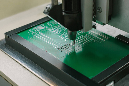
4.Drilling and Routing
5.Plating
The desired surfaces are coated with copper or other active materials to form circuit paths and through-hole plating. A lot of copper plating will be involved, and in many cases, it further requires processing, such as tin plating, to protect against oxidation.
6.Lamination
Multiple layers of PCB are clamped together with bonding under the heat and pressure effect. This epoxy resin is mainly used for the dielectric material between the insulation layers, providing comprehensive multi-layered support for complex circuitry.
7.Solder Mask and Legend Application
A protective solder mask is applied to the PCB to prevent short circuits and protect the traces from environmental damage.
The legend or silkscreen is added to show us where the components are supposed to be placed and replace designators, along with other valuable bits of information for assembly and debugging.
8.Electrical Testing
Electrical testing is done to ensure the completed PCB is functioning correctly and continually. It is tested in numerous ways, including automated optical inspection (AOI) and in-circuit tests, to ensure that the board meets all specifications and performs the intended function.
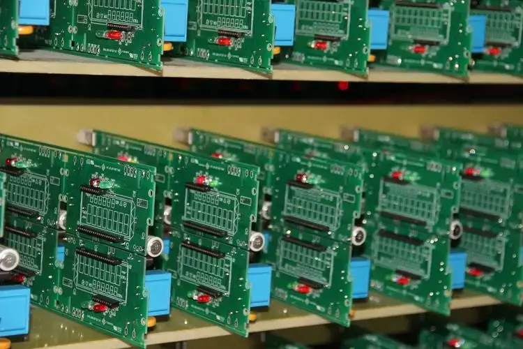
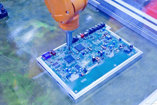
9.Assembly
The final step will be to attach electronic components to the PCB, either by SMT (surface mount technology) or through-hole soldering.
At the time of the original PCB assembly, a final test will be run to verify proper placement and operational condition for all components.
All of these steps are important for obtaining a PCB that is reliable and of good quality, according to the specific requirements of the intended application.
Understanding these steps provides valuable insights into the manufacturing process, helping you design and produce better, more efficient circuit boards.
Types of PCB Manufacturing
PCB manufacturing can be divided into flexible and rigid-flex boards, according to the rigidity of the boards and the complexity of the circuits.
Some of the more important among them are:
1.Rigid PCB Manufacturing
Rigid PCBs are the most commonly used ones in regular electronic devices. They are manufactured using solid, rigid material, for example, FR4 (a mixture of epoxy resin and glass fiber), which provides them with dimension and structural stability.
Such PCBs can be found in computers, television sets, and smartphones, where the board has to be fixed and rigid.
2.Flexible PCB Manufacturing
Flexible PCBs are designed for applications requiring bending or folding capabilities. They are built on substrates made of flexible plastic, typically polyimide. They allow the board to be bent, twisted, or conformed to shape.
This makes for such applications as wearables, flexible displays, and medical equipment, with products being a lot more versatile in design and function.
3.High-Density Interconnect (HDI) PCB Manufacturing
HDI PCBs are printed circuit boards for complex circuits with fine features and high layer counts. It includes better manufacturing techniques, thus making it feasible to place more components within the cards and give finer traces for the same.
Usually, HDI PCBs are used in advanced electronics such as smartphones, tablets, and military equipment, where high performance and compact size are very much desired.
These boards often feature micro vias, blind and buried vias, and high signal integrity to support sophisticated applications.
Understanding the various types of PCB manufacturing will enable you to choose the most appropriate type for your specific needs and consequently secure maximum performance and reliability for your electronic projects.
Now you know the basics of PCB manufacturing, it’s time to give you some tips that will help you in your project.
Additional Considerations in PCB Manufacturing
Beyond the basic manufacturing process and types of PCBs, several other important aspects influence the quality, efficiency, and cost of PCB production.
Here are some key considerations:
- Design for Manufacturability (DFM)
This is important for avoiding problems in the production process and for making the manufacturing process very smooth. DFM practices involve an optimization of PCB layout with the capabilities and constraints of the manufacturing process.
This may include proper spacing and alignment of components to minimize complex trace routes, along with material selection. Designers who are looking to prevent potential issues while reducing possible costs of production have to consider manufacturability.
- Quality Control
Quality monitoring at each stage of the PCB process ensures final board performance to prescribed specifications and quality. Several checks are in place at steps such as material inspection, photolithography, drilling, plating, and assembly.
Some methodologies ensure functionality, such as automated optical inspections, electrical testing, and in-circuit testing. Continuous control of quality enables early detection and subsequent correction of issues before they escalate into more significant problems in later stages of production.
- Cost and Pricing
Several factors affect the cost of PCB manufacturing, including material complexity, quantity, and specific production processes required.
Here is a general view of these factors:
- Complexity of Material: Better-quality materials, like Rogered or special lamination, can significantly affect cost compared to standard FR4.
- Number of Layers: Multi-layer PCBs are more expensive than single or double-layer boards due to additional materials and processing steps..
- Quantity:The cost per unit generally decreases for larger production runs due to the economies of scale.
- Design Complexity:Fine trace designs, small via designs, HDI designs, etc., require more sophisticated manufacturing, elevating the cost.
- Turnaround Time: Reduced production time can be costly compared to the regular lead times.
By noting such additional considerations, designers and engineers are well-poised to make informed decisions to optimize the process of manufacturing in terms of quality and cost management.
Conclusion
In conclusion, understanding PCB manufacturing is crucial for PCB designers, electronics engineers, and hobbyist. Knowing these steps will help you to design better and more efficiently while you can also make wise choices in your project.
Whether you are working on a simple gadget or a complex device, this knowledge will help you navigate the manufacturing process smoothly.