Are you a PCB designer finding high-speed PCB design a bit tricky? No worries! Understanding high-speed PCB design is like cracking a cool code to make your circuits work super-fast.
In this guide, we will make high-speed PCB design easy-peasy. From fixing signal stuff to nailing impedance, we have got your back.
So let’s get started.
What is High Speed PCB Design?
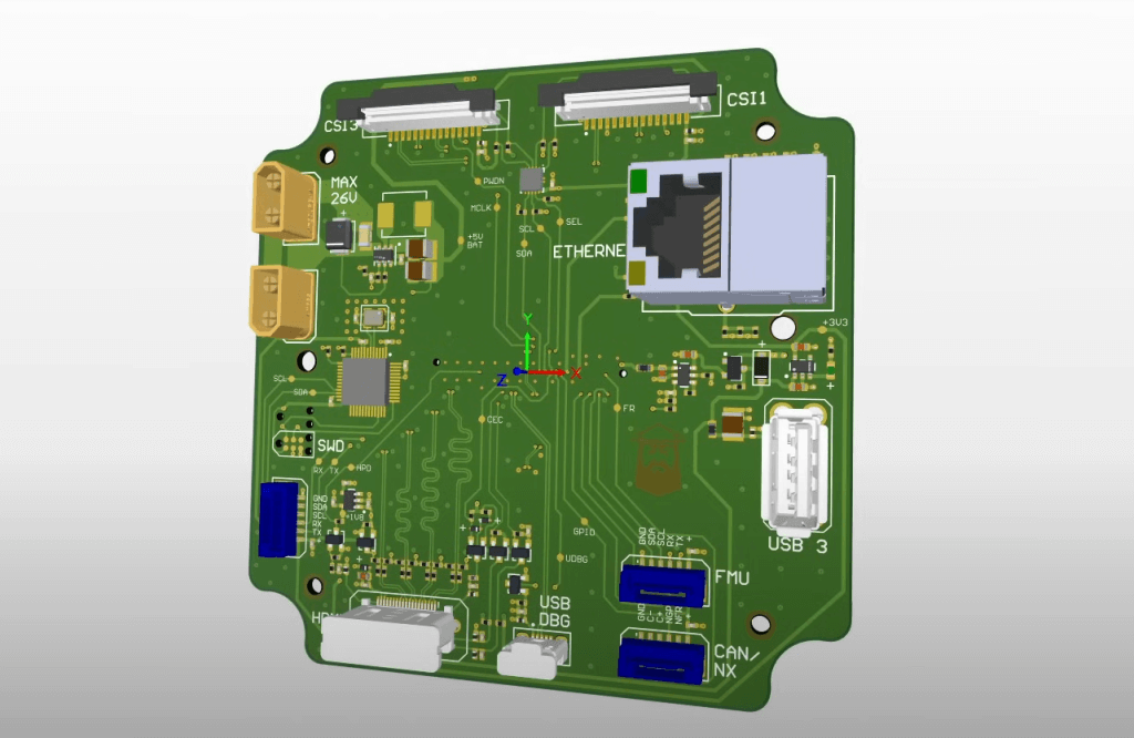
High-speed PCB design is the way of creating printed circuit boards optimized for circuits that operate at frequencies higher than a certain threshold, typically in the range of tens of megahertz (MHz) or even gigahertz (GHz).
These circuits are commonly found in applications such as computer motherboards, networking equipment, high-speed data acquisition systems, and telecommunications devices.
At its core, high-speed PCB design revolves around ensuring that signals can travel through the PCB without distortion or degradation, even at extremely fast speeds.
Now let’s discuss the unique challenges you can face in high speed PCB design.
Unique Challenges in High-Speed PCB Design
There are different challenges you might face during a high speed PCB designing process. The most important ones are:
- Signal Integrity
Maintaining signal integrity is crucial in high-speed PCB design. At elevated frequencies, signal degradation becomes a significant concern due to factors such as reflections, crosstalk, and the skin effect.
The skin effect causes the alternating current to flow near the surface of the conductor, leading to potential signal distortion and loss of data integrity.
- Electromagnetic Interference (EMI)
The risk of generating and being affected by EMI escalates with frequency. High-speed PCBs must be designed with meticulous attention to minimize EMI.
This is not only vital for the circuit’s performance but also to ensure it meets regulatory compliance standards.
- Controlled Impedance
Controlled impedance in PCB design is about ensuring that the board maintains a consistent impedance level to facilitate uniform signal propagation characteristics.
This is essential for the integrity of high-speed data transmission, preventing signal reflections and ensuring the reliability of the communication channel.

Comparison between High-Speed and Low-Speed PCB Design Approaches
Let’s take a closer look at how high-speed and low-speed PCB design approaches stack up against each other:
1. Trace Length
In high-speed designs, shorter is sweeter. Why? Longer traces in high-speed circuits can spell trouble, introducing signal loss and pesky reflections.
By keeping trace lengths to a minimum, you’re reducing the chances of signal degradation and ensuring smoother performance overall.
2. Trace Width and Spacing
Details matter in high-speed designs, especially when it comes to trace width and spacing. Why? Because these factors directly impact impedance and crosstalk.
By meticulously optimizing trace widths and spacing, you’re maintaining signal integrity and keeping interference at bay, ensuring your circuit runs like a well-oiled machine.
3. Multilayer PCBs
With multiple layers and strategic placement of power and ground planes, you’re boosting signal integrity and taming noise.
These extra layers act as shields, shielding your signals from interference and providing a stable environment for your circuit to thrive.
4. Advanced Routing Techniques
For the seasoned pros, advanced routing techniques like differential pairs and smart component placement are where the magic happens.
Differential pairs help tame electromagnetic interference, while clever component placement cuts down on signal path lengths and minimizes pesky parasitic effects.
Signal Integrity and High-Speed Design
Maintaining signal integrity is the cornerstone of successful high-speed PCB design. Let’s delve into how signal degradation can occur and explore some key design techniques to ensure optimal signal quality:
Signal Degradation
Imagine your signal as a traveler on a highway, cruising along at high speeds. But along the way, it encounters obstacles like reflections, crosstalk from neighboring signals, and the skin effect, where high-frequency signals tend to travel near the surface of conductors. These hurdles can distort the signal, leading to potential bit errors or even complete malfunctions in your circuit.
Design Techniques for Signal Integrity
- Controlled Impedance Routing:Think of controlled impedance routing as creating a smooth, paved road for your signals. By carefully selecting trace geometries and materials, you ensure consistent impedance throughout your PCB, minimizing signal reflections and distortions.
- Proper Termination Techniques:Just like guiding traffic, proper termination techniques help signal transitions flow smoothly. Techniques like series termination and parallel termination prevent signal reflections by matching the impedance at the end of the transmission line, ensuring signals reach their destination without bouncing back.
- Minimizing Via Usage:Vias, while essential for routing signals between layers, can also introduce impedance mismatches and signal reflections. Minimizing via usage, especially for high-speed signals, reduces these impedance variations and helps maintain signal integrity.
By implementing these design techniques, you’re not just preserving signal integrity – you’re paving the way for reliable, high-performance circuits that meet the demands of today’s fast-paced electronic applications.
Conclusion
In conclusion, mastering high-speed PCB design is essential for creating reliable, high-performance circuits. From understanding the unique challenges to implementing advanced design techniques, this guide has equipped you with the knowledge and tools to tackle high-speed PCB design with confidence.


