


Are you struggling to maintain signal integrity in your electronic designs? Of course, you are not alone, and most people find it a bit complicated to handle high-frequency PCBs.
The developers of these unique boards require them to work on signals with ranges from hundreds of megahertz to tens of gigahertz while being similar in design and fabrication.
But do not worry, since in this article, we will discuss everything you need to know, from materials and design considerations to real-world applications regarding high-frequency PCB requirements.
What is High Frequency PCB?
As you know, a PCB is nothing more than a simple piece that constitutes one of the most straightforward bases of modern electronics. It is a board used for mechanically supporting and electrically connecting electronic components by the use of conductive pathways that are etched from copper sheets laminated onto the surface.
PCBs are the units that provide structure and help support the smooth transmission of electrical signals interfacing among various electronic active and passive devices.
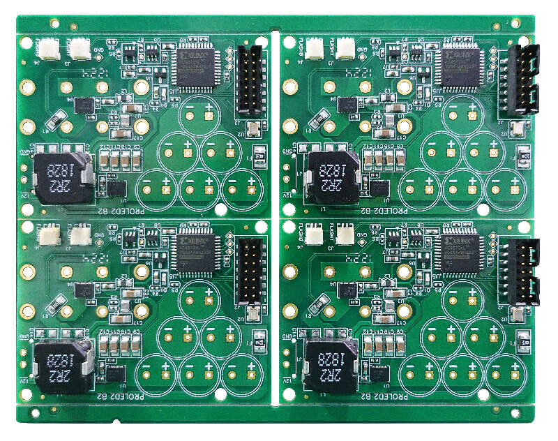
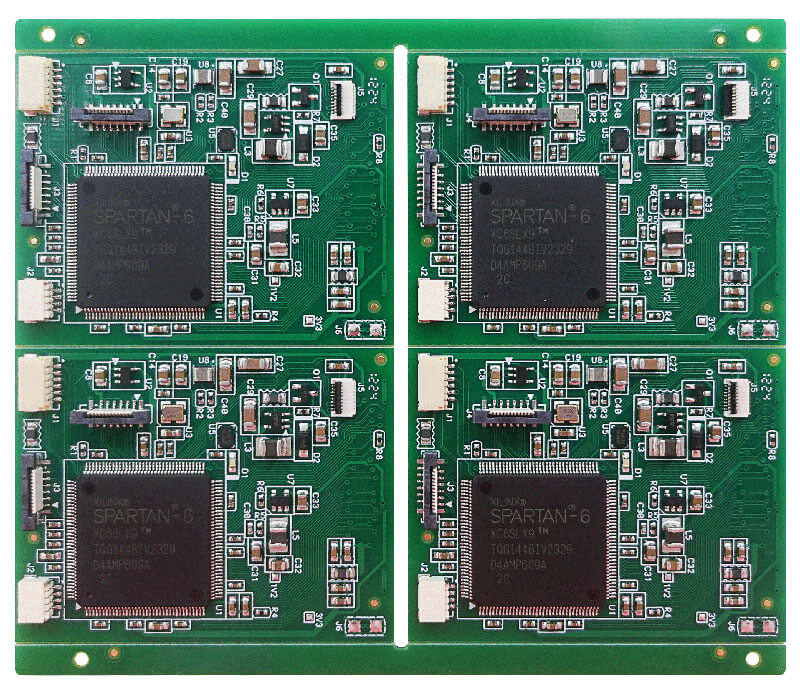
The high-frequency PCBs are, therefore, by name, a particular type designed to handle high-frequency signals that may even work in the range from hundreds of megahertz (MHz) to tens of gigahertz (GHz).
These are standard frequencies for applications in telecommunication, radar, wireless communication devices, and high-speed digital circuits.
The difference between High-Frequency PCBs and standard PCBs lies in their construction and materials. High-Frequency PCBs are engineered with specific design considerations and materials optimized to minimize signal loss, impedance mismatch, and electromagnetic interference (EMI) at high frequencies.
Standard PCBs, while suitable for many electronic applications, are not well-suited for high-frequency signals due to several factors:
- Signal Degradation: Attenuation increases at higher frequencies in traveling signals on the conductive traces of a PCB. This, in effect, can lead to dramatic decreases in signal strength and, hence performance of the electronic system.
- Impedance Mismatch:In other words, high-frequency signals need components to be matched with the transmission lines properly to connect between them so that the resultant reflectance of the signals is minimal, and so is the maximum power transfer that it supports. And the standard PCB materials and fabrication techniques are not up to the level of impedance control that high-frequency applications require.
- EMI and Crosstalk:EMI and crosstalk come into play with higher frequencies because of signal stretching, and they cross with neighbor components on the board. High-Frequency PCBs employ specialized design techniques and materials to minimize EMI and crosstalk effects.
So, high-frequency PCBs allow for advanced signal integrity, impedance control, and EMI performance in applications where a High-Frequency PCB is developed, and not just a standard PCB.
Additionally, the specialization in design and construction permits the proper handling of respective challenges from signals at operating frequencies that are considerably high.
Now let’s get to know about the materials for high frequency PCBs.
Materials for High Frequency PCBs
FR4, the standard material used in PCB fabrication, has limitations at high frequencies primarily due to its dielectric constant and loss tangent.
The dielectric constant is an index representative of the material’s ability to support stored electrical energy when an electric field is exposed. However, because of material characteristics with field deformability at high frequency, a signal distortion and impedance mismatch are created, decreasing the signal integrity for FR4.
Additionally, the loss tangent of FR4, which measures the dissipation of energy as heat, increases at higher frequencies, resulting in higher signal attenuation.
To address these limitations, alternative high-frequency materials are utilized in PCB manufacturing:
1.FR-406/FR-480
These materials are more advanced than FR4, possessing a much lower dielectric constant than the regular FR-4.
The dielectric constant has been brought low through these materials to reduce signal distortion at higher frequencies, thereby reducing impedance variations to get better propagation of signals with better impedance control eventually.
2.Rogers
Rogers Corporation manufactures superior materials for the making of, among other things, ceramic-filled laminates and high-frequency organic laminates.
Technically, the electrical properties of these materials are very appealing: ultra-low dielectric loss, a very stable dielectric constant over a wide frequency band, and thermal stability.
This venerable suite of materials brings its legacy in convincing design engineers of the need for Rogers specifications for design applications that require precise control over impedance and low losses in signal processing.
3.Polyimide
As you may know, polyimides are highly flexible materials with good performance at high frequencies because of their low dielectric loss and excellent thermal stability, which makes them suitable for high-flex circuit applications, such as wearable electronics, aerospace, and automotive radar systems.
And the choice of material significantly impacts various aspects of PCB performance including signal propagation, impedance control, and thermal stability. That is why it is important to choose the right material when it comes to high-frequency PCBs.
Design Considerations for High Frequency PCBs
In high-frequency PCB designs, signal integrity measures the system’s high frequency to prevent signal impairments and errors that may cause deterioration in the performance of high-frequency systems.
Several key design considerations play a crucial role:
- Impedance Control: Impedance control is necessary so that the width and spacing of traces can remain unaltered; therefore, the signal may adequately be carried, and deviations in the impedance along the signal paths may be guarded.
- Controlled Impedance Routing Techniques: Employing techniques like microstrip lines and stripline structures helps maintain controlled impedance, crucial for minimizing signal reflections and ensuring optimal signal integrity.
- Minimizing Crosstalk: The spacing and shielding of signal traces are designed very carefully so that undesirable signals couple with one another or poorly attenuated signals skip over others. In some cases, this could even encourage the flow of signal crosstalk and noise.
- Grounding and Power Distribution: Proper distribution of power networks and relying on a large plane for ground are essential not only to reduce ground bounce and voltage noise but to ensure good signal integrity on large scales.
- Via Placement and Types: Signal distortion can be kept to a minimum by making use of the proper placement and selection of high-frequency via structures and maintaining signal integrity. Minimizing via usage where possible and utilizing high-frequency via types help mitigate signal degradation caused by vias.
So, these aspects of the design have to be given top consideration to realize signal integrity optimization in an HF PCB interfacing stringent applications.
Now you know the basics of high frequency PCBs, it’s time to discuss the their manufacturing process and the challenges in detail.
Manufacturing Process and Challenges
The basic manufacturing process for high-frequency PCBs involves several key steps: lamination, etching, and drilling.
Lamination begins with layering substrate materials and bonding them together under heat and pressure to form the base PCB.
Next, the circuit pattern is defined through etching, where a chemical solution removes unwanted copper from the substrate, leaving behind the desired conductive traces.
Finally, holes for component mounting and interconnectio n are drilled into the PCB using advanced drilling techniques.
However, compared to standard PCB manufacturing, high-frequency PCB fabrication presents specific challenges:
- Tighter Tolerances: High-frequency printed circuit boards are expected to have closed tolerances in trace width, spacing, and dielectric constants to ensure signal integrity and impedance control. However, it is pretty challenging to maintain such tolerances in the manufacturing process.
- Advanced Drilling Techniques: High-frequency PCBs should use advanced drilling techniques, often with laser drilling or controlled depth drilling, to realize vias with minimal signal loss distortion, and impedance variation. These need specialized equipment and skills to do this carelessly, so the associated manufacturing process is quite complex.
- Material Handling: Because the material is handled at higher frequencies, it is much more sensitive to delicate handling compared to common PCB materials. Mechanical stress must be kept at a minimum level, and storage conditions must use nature-friendly material, thereby avoiding, best in a manner, any spoilage of the material.
So, such problems must be considered at the manufacturing stage of high-frequency PCBs so that the integrity and functionality are held at their best to meet high-frequency applications with tight requirements.
Applications of High Frequency PCBs
If you are wondering where does high frequency PCBs are used, here are some common applications:
1.Radiofrequency (RF) Communication Devices
High-frequency PCBs are very important in constructing mobile phones, Wi-Fi routers, Bluetooth modules, and other types of wireless communication tools.
This is highly illustrative since the PCBs present can serve for the transmission and reception of RF signals into good operating conditions and information exchange of modern wireless communication networks.
2.High-Speed Computer Components
High-frequency PCBs are essentially the inside demand of a high-performance computing system. In this regard, high-frequency boards can support the high-speed data buses applied when interfacing motherboards and DDR memory interfaces with devices, for instance, PCIe and graphic cards, respectively.
Therefore, they influence not only the overall performance but also the system response in general by enabling the data interchange between different components at very high speeds.
3.Microwave and Radar Systems
High-frequency PCBs are fundamental in microwave and radar systems used in various applications, including aerospace, defense, and automotive industries.
These PCBs enable the precise transmission and reception of high-frequency electromagnetic signals, essential for radar sensing, communication, and navigation.
4.Test and Measurement Equipment
High-frequency PCBs are applied in test and measurement equipment. To name a few: oscilloscopes, spectrum analyzers, and network analyzers.
In the research, development, and quality control phases, they enable signal integrity and precision to reach an exact measurement and analysis of high-frequency signals.
Final Words
In conclusion, high-frequency PCBs are essential for ensuring reliable signal transmission in electronic devices operating at elevated frequencies, from telecommunications to radar systems.
By understanding everything about them, engineers can effectively overcome challenges and harness the benefits of high-frequency PCBs.