


Have you just heard about heavy copper PCB and now you are wondering what is it? Or are you an electronics engineer or a PCB designer looking to learn more about heavy copper PCBs? If yes, you are on the right page as here we are going to discuss everything you need to know about heavy copper PCB.
By going through this guide, you will be well-equipped with what is heavy copper PCB, its properties, applications, design considerations, and more.
So, let’s get started.
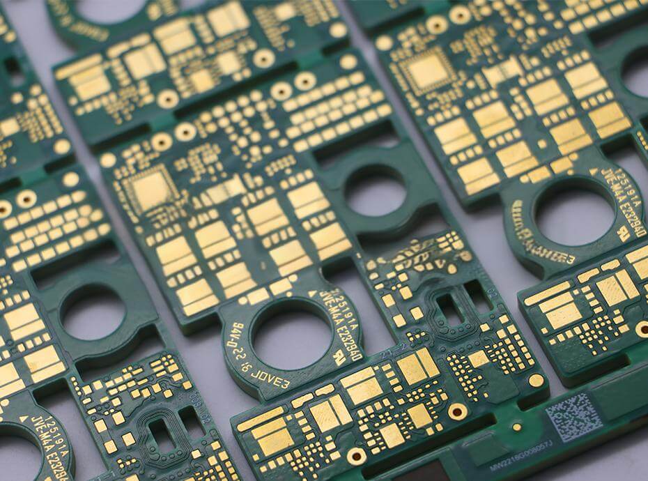
What is Heavy Copper PCB
As everyone knows, a PCB is the backbone of electronic devices, providing platform support to mount the electronics components.
These boards are made by stacking up a layers of some conductor—usually copper—to form complex paths known as traces. These traces act like electrical highways along which signals can pass between components to realize the function of the circuit.
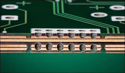
But what is a heavy copper PCB? Unlike their standard counterparts, heavy copper PCBs boast copper layers of greater than 3 ounces per square foot in thickness. This additional copper mass unlocks a plethora of benefits, ranging from increased current-carrying capacity to enhanced thermal management.
The heavy copper PCBs are the superheroes of the electronic world in that they can easily handle high-power applications.
Properties of Heavy Copper PCBs
There are different characteristics of heavy copper PCBs that make them suitable for multiple applications:
1.Increased Current Carrying Capacity
Heavy copper PCBs have thicker layers of copper, allowing electrons to flow with less resistance. In this way, heavy copper PCB modules support high current values without any harm from heat.
Whether power converters, motor drives, or other high-power electronic requirements, heavy copper PCBs help ensure that the electricity flow is seamless, providing top-notch performance every time.
2.Reduced Power Loss
Such PCBs have strengthened layers of copper and, therefore, reduce resistance significantly so that there is minimal loss of energy during current transmission. The result is an electrical system that is efficient, robust and maximizes energy use while causing little waste.
3.Improved Heat Dissipation
Heavy Copper PCBs are supreme when it comes to the management of heat in electronics. The extra mass accompanying copper operates as a heatsink, pulling heat away from sensitive components and disseminating it into the surrounding environment.
This not only prevents overheating but also ensures prolonged durability and reliability of the electronic system.
Be it LED lighting systems, power amplifiers, or industrial control systems, heavy copper PCBs keep components cool under pressure.
But where are heavy copper PCBs used? What are the common applications? Let’s discuss this in detail.
Applications of Heavy Copper PCBs
Heavy copper PCBs find their niche in a wide array of real-world applications where their exceptional current handling capabilities are indispensable:
- Power Electronics
Inverters, converters, and motor drives demand heavy copper PCBs to effectively manage the high currents required for their operation. Heavy copper PCBs ensure reliable performance and prevent overheating in these power-intensive applications.
- LED Lighting Systems
LED driver circuits require heavy copper PCBs to handle the high currents that are needed to power LEDs. Heavy copper PCBs are highly necessary for efficient energy transfer concerning LED lighting systems, which facilitate the process.
- High-Performance Audio Equipment
Power amplifiers in high-performance audio equipment benefit from heavy copper PCBs to deliver clear and distortion-free sound. Heavy copper PCBs can bear strong currents, which ensures high efficiency of power supply and, henceforth, the best audio.
- Industrial Automation and Control Systems
Heavy copper PCBs are used for power distribution units and motor controllers in the industry, where high currents are expected. They supply the reliability and robustness demanded by industrial automation and control systems under increasingly severe conditions.
This means that heavy copper PCBs are preferred in such applications, as they can withstand very heavy currents. Thus, their performance is assured to be reliable and long-lasting in even the most demanding environments.
Heavy Copper vs. Standard Copper PCBs
If we compare the attributes of heavy copper to normal copper PCBs, we can say that:
|
Property
|
Heavy Copper PCBs
|
Standard Copper PCBs
|
|---|---|---|
|
Current Rating
|
Higher due to thicker copper layers
|
Lower
|
|
Power Loss
|
Reduced due to lower resistance
|
Higher
|
|
Thermal Performance
|
Better heat dissipation
|
Less efficient heat dissipation
|
|
Cost
|
Higher due to increased material and processing requirements
|
Lower
|
|
Weight
|
Heavier, which may be a concern in weight-sensitive applications
|
Lighter
|
|
Manufacturability
|
Requires specialized tooling and expertise for drilling and routing
|
Standard processes apply
|
Trade-offs:
- Cost:Heavy copper PCBs sometimes offer significantly improved performance but are more expensive to fabricate due to added requirements, such as the material and processing.
- Weight Considerations: Heavy copper PCBs will weigh more than standard PCBs; this can sometimes be problematic for weight-sensitive applications, such as aerospace applications, where every ounce counts.
- Manufacturability challenges: Since heavy copper PCBs have thicker copper features, the drilling and routing processes require specialized tooling and expert knowledge. This often can mean additional costly production time compared to a standard PCB.
Heavy Copper PCB Design Considerations
The designing of heavy copper PCBs involves proper consideration of some critical factors that make sure they perform well and are reliable:
1.Current Rating Calculations
It’s crucial to accurately determine the required current capacity of the PCB to select the appropriate copper thickness.
Thicker copper layers will give higher current-carrying capability, but the ability must align with the application’s need to prevent hazardous overheating and guarantee safety.
2.Heat Dissipation Strategies
Dismembering enough heat is important to keep the electronic components away from thermal problems and for general longevity. Designers should, therefore, plan for effective heat transfer through means that can be applied, such as using heatsinks or thermal vias in a given PCB layout.
These elements will help dissipate heat from high currents flowing through copper traces, allowing average working temperatures.
3.Electromagnetic Interference (EMI) Considerations
The extra thickness of copper in heavy copper PCBs can also give them some inherent EMI shielding properties, thus lessening the possibilities of emitting interference with nearby electronic devices.
Depending on the application’s sensitivity to EMI, other observable measures within the applications would, therefore, be necessary given practical observation of potential interference issues.
Designers must, thus, carefully evaluate application EMI requirements and take suitable measures in the PCB design to ensure reliable application performance.
4.Mechanical Strength
The mechanical strength of the heavy copper PCBs can further be improved by increasing the thickness of the copper layers. It becomes beneficial, especially for the application in which the PCB will be exposed to mechanical stress or vibration.
Designers should look at the mechanical needs of a specific application and select appropriate thickness levels in heavy copper PCBs to assure durability and reliability in rugged environments.
5.Plated Through Holes and Trace Width
When designing heavy copper PCBs, special attention should be given to plated through holes and trace width.
As a rule, the thicker copper layer will require adjustment in the size and depth of the plated through holes to ensure that the conductivity is correct and the reliability is perfectly okay. Trace width, on the other hand, should also be optimized in such a way as to accommodate the higher currents yet maintain the proper spacing to minimize electrical interference and ensure signal integrity.
These considerations allow designers to design heavy copper PCBs with due diligence so that all requirements of applications are met while optimum performance and reliability are sustained.
Conclusion
In conclusion, heavy copper PCBs are a game-changer in the world of electronics. They cater to high currents at the same time, reduce power loss, and enhance heat dissipation, making them applicable in a variety of applications, from power electronics to industrial automation.
They come with some trade-offs, like high cost and weight issues, but the benefits certainly outweigh the challenges. By carefully considering the design factors given above, engineers can utilize the full potential of heavy copper PCBs for their needs in producing rugged and reliable electronic systems.