


Are you wondering what a footprint in PCB design is all about? Searching on the internet to learn everything about footprint in PCB design? No need to stress as this article aims to help you understand exactly what footprints are and why they are important to your PCB projects.
By the end of the article, you will be all clued in on how footprints work and why they are super important.
So, let’s get started.
What is the Footprint in PCB Design
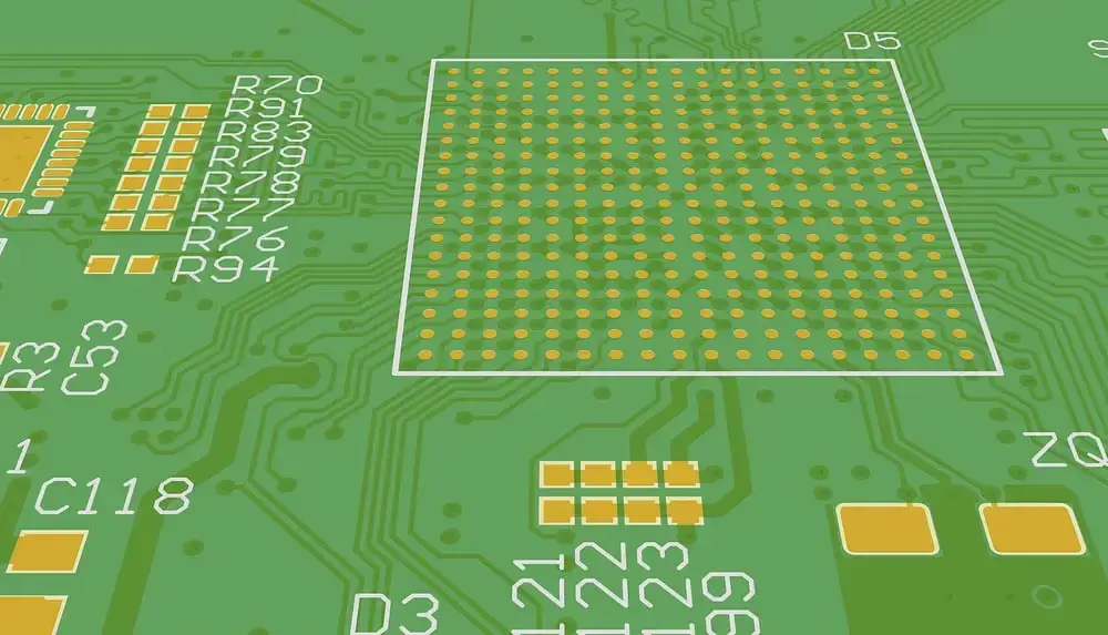
In PCB design, a footprint refers to a unique arrangement of pads, vias, and reference designators on the board that outline the area where a component is attached via soldering.
This is what basically forms the physical interface between the electronic component and the PCB. A good footprint design gives an impression of the physical dimensions and pin configuration of the component it is meant to accommodate.
It ensures that each of the components is properly aligned in a right position on the circuit board, which results in proper electrical connectivity and mechanical stability.
These are footprints that contain metal pads, on which the component leads make solder contact to form the interconnections. Vias are small plated-through holes in the PCB that facilitate interconnections between different layers of the board.
Reference designators, on the other hand, are alphabetic tags for uniquely identifying PCB components, usually for aiding in the course of assembling and finding faults.
Now, let’s try to understand why footprints are important when designing for PCB.
Why Footprints Are Essential in PCB Designing
As said above, footprints are essential for various components like:
1.Resistors and Capacitors
Resistors and capacitors are the most basic components of an electronic circuit, and their footprints need to be placed properly to ensure the effective soldering and placement of these components.
Both are made up of pads that are properly aligned with the leads of the resistor or capacitor for a firm connection to the PCB. Proper pad size and clearance are required to avoid soldering issues and ensure proper connections.
2.Integrated Circuits (ICs)
Integrated circuits are Small semiconductor devices of many electronic components in one package. IC footprints are designed to make the package type and pin configuration of an IC.
This literally involves a proper pad layout and spacing to the IC’s pin arrangement, hence ensuring a good soldering and electrical connection.
3.Connectors
Connectors are component footprints designed to provide electrical connections between PCBs, or between a PCB and a device. A footprint pattern is defined as a connector if it has pads or pins in a pattern to reflect the pattern of the connector contacts.
The most important part is correct alignment and spacing of these pads to allow for reliable connections and to cut down on signal interference.
4.Other Components
In addition to integrated circuits, footprints are also used in many other components that make their way into a PCB design: diodes, transistors, switches, and so on.
Each will have its own footprint matched with the package type and pin configuration. Representing the physical dimensions and layout of those components on the PCB allows efficient assembly and ensures the optimal performance of the circuit.
Selecting the Right Footprint
Selecting the right footprint for a component is a crucial step in PCB design, as it directly impacts the performance and functionality of the circuit.
Here’s how you can effectively choose the appropriate footprint:
1.Considerations for Component Selection
When selecting a footprint for a component, several factors need to be taken into account:
- Package Type: Different components come in various package types, such as surface mount (SMD), through-hole, or ball grid array (BGA). The footprint must match the specific package type of the component.
- Pin Count: The number of pins or leads on the component determines the layout and size of the footprint. Ensure that the footprint provides enough space and proper arrangement for all pins to be soldered onto the PCB.
- Component Size: The physical dimensions of the component, including length, width, and height, must be considered when selecting the footprint. The footprint should accommodate the component’s size without overlapping neighboring components or exceeding board dimensions.
2.Package Compatibility
Verify that the selected footprint is compatible with the component’s package specifications. This includes matching pad sizes, pad spacing, and pad layout to ensure proper soldering and electrical connections.
3.Industry Standards and Guidelines
Refer to industry standards and guidelines, such as IPC-7351 or manufacturer datasheets, for recommended footprint dimensions and layouts. Adhering to these standards helps ensure compatibility with assembly processes and enhances overall reliability.
4.Simulation and Testing
Utilize simulation tools or PCB design software to verify the compatibility and performance of the selected footprint. Conducting simulations can help identify any potential issues or optimizations needed before proceeding with PCB fabrication.
5.Flexibility and Adaptability
Choose footprints that offer flexibility and adaptability for future design iterations or component substitutions. Design footprints with standard pad layouts and clearances to facilitate easy replacement or upgrades of components without requiring significant redesign efforts.
By carefully considering these factors and guidelines, you can confidently select the right footprint for each component in your PCB design, ensuring optimal performance, reliability, and manufacturability.
So now you must be wondering what tools they use to create footprints. Let’s discuss this in detail.
Footprint Creation Tools and Resources
Creating footprints for components in PCB design can be made easier with the help of various tools and resources available in PCB design software.
Let’s take a closer look at some of these tools:
- PCB Design Software
PCB design software, like Eagle, KiCad, or Altium Designer, often includes built-in tools for making footprints. These tools let designers create custom footprints or choose from a library of ready-made ones. You can adjust things like pad sizes and spacings to fit your component perfectly.
- Footprint Libraries
In these software programs, you’ll find libraries full of pre-made footprints for common components. It’s like having a collection of blueprints ready to go. You just need to pick the right one for your component, saving you time and effort.
- Manufacturer Resources
Component manufacturers, such as Texas Instruments or Analog Devices, often provide footprint libraries or guidelines on their websites. These resources give you footprints tailor-made for their components, ensuring a perfect fit and compatibility.
- 3D Modeling Tools
Some advanced PCB design software, like Autodesk Fusion 360, offers 3D modeling features. These tools let you create realistic 3D models of your footprints, so you can see how components will fit on your board before you even start soldering.
With these tools at your disposal, creating footprints for your PCB designs becomes a much simpler and more efficient process.
Conclusion
In wrapping up, footprints are like maps for PCB design, guiding where components are soldered onto the board. From resistors to connectors, each part relies on a well-designed footprint for the right fit and connection.
By understanding footprints’ importance and using these tools, designers can improve their PCB designs’ performance and reliability.