


Are you also puzzled about what fanout really means in PCB design? Well, worry not, you are not alone as navigating the complexities of PCB layout can be daunting, especially when it comes to ensuring efficient signal transmission and minimizing signal integrity issues.
But don’t worry; this complete guide has you covered. Let’s break down what fanout means in PCB design and how it can be your secret weapon to optimize circuit board layouts.
So, let’s get going.
What is a Fanout in PCB design
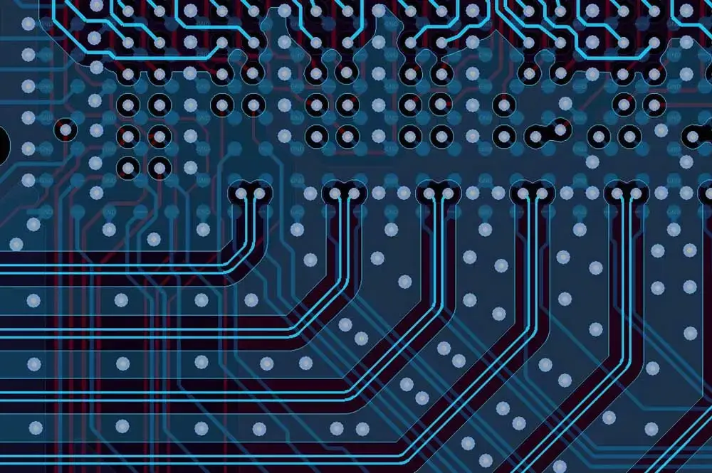
Fanout is a PCB design technique that allows a single output pin of a component to fan out to multiple input pins of other components. It involves placing short traces and vias, which in essence are a mode of electrical conduction.
Essentially, fanout is a technique that is aimed at improving the distribution of signals across a circuit board, making communication between various components possible and much better.
Consider a microcontroller, which has many output pins to communicate with peripheral devices. If there were no fanout, you would have to run all the traces from each individual output pin to its corresponding input pin on each device. That would make for a very ugly and ineffective layout.
However, by employing fanout techniques, you can streamline the routing process and optimize signal transmission.
But what are the advantages of Fanout? Let’s discuss this in detail.
Benefits of Fanout
Fanout brings many key advantages that enhance the performance and efficiency of PCB designs.
1.Improved signal integrity:
As mentioned earlier, by the use of fan-out technique, signal integrity is further improved through the minimization of trace length. This shortens the trace, thus ensuring a reduction in potential signal degradation, impedance mismatches, and electromagnetic interferences.
In other words, it assures that the communication between components is assured.
2.Signal Routing Based on an Efficient Algorithm:
Fanout is the concept through which signals are efficiently routed. So, if the pin count is high, the said purpose is served very well.
Routing traces from each pin is replaced by fanout, so that a number of pins have a common routing path. This is a way through which simplification in the layout and reduction in routing congestion are achieved very easily.
3.Better accommodation of tightly spaced pins:
In modern electronics, components with closely spaced pins, such as fine-pitch BGAs, pose layout challenges.
Fanout techniques enable designers to effectively route signals from densely packed components, optimizing board space utilization without compromising signal integrity or manufacturability.
So now that you are well informed about the very basics of Fanout in PCB design, it is time to discuss why one should use Fanout.
Necessity of Fanout in PCB Designing
Fanout is essential in several typical scenarios in PCB design, particularly when dealing with high-density integrated circuits (ICs) like Ball Grid Arrays (BGAs).
Here’s why:
- Ball Grid Arrays (BGAs):
BGAs are notorious for their high pin count and compact footprint, making traditional routing methods impractical. Fanout becomes necessary to efficiently route signals from the densely packed array of solder balls on the underside of the BGA package to the rest of the PCB.
Without fanout, achieving signal connectivity for each individual pin would be extremely challenging and result in a cluttered and congested layout.
- High-Density Integrated Circuits (ICs):
Beyond BGAs, many modern ICs feature high pin counts and fine pitch configurations. These ICs are commonly found in applications such as microcontrollers, FPGAs, and ASICs.
Fanout is crucial for these components to ensure that signals can be routed efficiently and reliably between the IC and other circuitry on the PCB.
Without fanout, the complexity of routing individual traces for each pin would be overwhelming, leading to routing congestion and potential signal integrity issues.
So, fanout is necessary in PCB design, particularly when dealing with components like BGAs and high-density ICs, to enable efficient signal routing and ensure the reliability and performance of the electronic system.
Different Fanout Routing Styles
There are several fanout routing styles commonly used in PCB design, each with its own advantages and considerations:
- Teardrop Routing:Teardrop routing involves widening the trace at the junction where it meets the via or pad, resembling a teardrop shape. This style helps to improve reliability by reducing the risk of copper cracking at the junction. Teardrop routing is particularly useful in high-reliability applications or environments where mechanical stress is a concern.
- Dog-Bone Routing:In dog-bone routing, the traces extend from the pad to the via in a straight line, and then a short stub is added perpendicular to the trace to connect it to the via. This style is effective for minimizing signal reflections and impedance mismatches, especially in high-speed digital designs. Dog-bone routing also provides additional copper area for soldering, enhancing the strength of the connection.
- Hidden Via Approach:The hidden via approach involves burying vias underneath components, rather than having them exposed on the surface of the PCB. This style helps to maximize board space utilization and improve the overall aesthetics of the PCB. However, hidden vias may require additional manufacturing steps and increase fabrication costs.
By understanding and selecting the appropriate fanout routing style, designers can optimize signal integrity, reliability, and manufacturability in their PCB designs.
Conclusion
So that’s all you need to know about fanout in PCB design. With the knowledge gained from this guide, you are now equipped to tackle even the most complex PCB layouts with confidence.
So go ahead, unleash your creativity, and design PCBs that push the boundaries of innovation and excellence.