


Do you find it difficult to maintain signal integrity in your PCB designs? The solution may lie in the understanding of the power of differential pairs. Now consider for a second: you’ve made your PCB layout, but somehow noise and interference seem to come from everywhere, causing bad performance on your design. Fear not, because this article is here to help you.
We will first walk through the world of differential pairs in PCB design, understand the importance of those, and finally provide practical solutions so that your signals make a good and smooth trip to their destination.
So let’s get started.
What is a Differential Pair in PCB Design?
A differential pair in PCB design is a system of two parallel conductive tracks on a circuit board that has an equal but opposite relationship in magnitude to each other. So, when one signal is high, the other has to be low, and vice versa.
This type of configuration of signals makes it very resistant to all kinds of external noise and electromagnetic interferences, since any noise picked up by the tracks tends to be common to both, and hence gets cancelled out by the receiving circuitry.
Differential pairs are very important for signal integrity with respect to high-speed digital circuits applied in systems like USB, Ethernet, or HDMI.
The differential pair is maintained in a constant spacing and parallel routing, making the time for signals to travel down the tracks the same. This is important for data integrity.
Now, let’s look at the key advantages of using differential pairs over single-ended signaling.
Key Advantages of Using Differential Pairs Compared to Single-Ended Signaling
There are many advantages to using differential pairs over single-ended signaling.
Let’s discuss the most important ones in detail:
1.Improved Noise Immunity
In PCB design, noise is a persistent challenge that can distort signals and degrade performance. With a differential pair, however, the equal but opposite signals effectively combat common-mode noise.
This means that any noise picked up by the traces affects both signals similarly. At the receiving end, the circuitry can then differentiate between the intended signal and the noise, effectively filtering it out.
This inherent noise-cancellation property significantly enhances the immunity of the signals to external disturbances, ensuring that the transmitted data remains accurate and reliable, even in noisy environments filled with electromagnetic interference.
2.Reduced EMI (Electromagnetic Interference)
Electromagnetic interference (EMI) can disrupt the operation of electronic devices and compromise signal integrity. By utilizing differential pairs, designers can mitigate the effects of EMI significantly.
Since common-mode noise is cancelled out in the receiving circuitry, there’s less susceptibility to external electromagnetic fields. This reduction in EMI not only improves the performance of the specific PCB but also minimizes the potential for interference with neighboring components or systems.
It ensures that the signals remain clear and stable, even in environments where electromagnetic interference is prevalent, such as industrial settings or areas with high radio frequency activity.
3.Higher Signal Integrity
Signal integrity refers to the reliability and accuracy of transmitted signals, particularly in high-speed digital circuits where timing is critical. In a PCB design, maintaining consistent signal integrity is paramount to ensure data is transmitted correctly.
Differential pairs excel in this aspect by ensuring that signals propagate with minimal distortion. The parallel routing and consistent spacing of the conductive traces in a differential pair ensure that both signals arrive at the receiving end simultaneously.
This minimizes timing skew and signal distortion, allowing for reliable data transmission even at high speeds. The result is a PCB design that can effectively handle high-frequency signals without sacrificing accuracy or introducing errors, making it ideal for applications such as high-speed data communication and digital signal processing.
Overall, the advantages of differential pairs over single-ended signaling boil down to their teamwork mentality—they’re the dynamic duo that tackles noise, EMI, and signal integrity issues head-on, ensuring your PCB designs operate at their peak performance.
Now you know the basics of differential pair in PCB design, it’s time to learn it’s working principle.
Working Principle of Differential Pairs
The working principle of a differential pair in PCB design revolves around the coordinated operation of driver and receiver circuits.
Here’s how each component contributes to the functionality of a differential pair:
1.Driver Circuits
At the heart of a differential pair are the driver circuits, responsible for generating the equal but opposite signals that flow through the pair of conductive traces. These driver circuits typically consist of complementary transistors or amplifier stages configured to produce signals that mirror each other’s voltage levels but differ in polarity.
When a digital signal needs to be transmitted, the driver circuits generate these complementary signals and feed them into the corresponding traces of the differential pair.
The precise timing and voltage levels of these signals are crucial for maintaining signal integrity and ensuring accurate data transmission.
2.Receiver Circuits
On the receiving end of the PCB, the differential signals are fed into receiver circuits designed to extract the original data from the transmitted signals. The receiver circuits must be able to differentiate between the two complementary signals and effectively amplify and process the desired signal while rejecting common-mode noise and interference.
Typically, receiver circuits include differential amplifiers or comparators that analyze the voltage difference between the two signals in the pair.
By comparing the voltage levels of the two signals, the receiver circuits can reconstruct the original data with high accuracy, even in the presence of noise or distortion.
Overall, the working principle of a differential pair relies on the coordinated operation of driver and receiver circuits to transmit and receive signals with high fidelity and reliability.
By generating complementary signals and leveraging the differential signaling scheme, differential pairs enable robust communication in high-speed digital circuits while minimizing the effects of noise and interference.
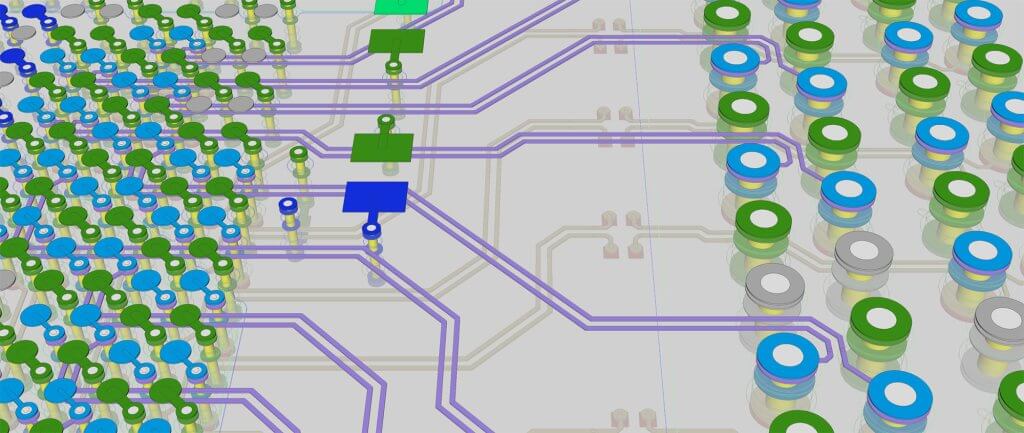
Practical Tips for Routing Differential Pairs
As said above, routing differential pairs correctly is crucial for maintaining signal integrity and minimizing electromagnetic interference in PCB designs.
So here are some practical tips for routing these pairs effectively:
- Matched Length
Ensuring that the traces of the differential pair are precisely matched in length is essential for maintaining signal timing and integrity. Any mismatch in length between the two traces can introduce skew, leading to signal distortion and potential errors.
Use PCB design software with length-matching features to route the traces with precision, adjusting their lengths as necessary to achieve perfect alignment.
- Controlled Impedance
Differential pairs require controlled impedance to maintain signal integrity and minimize reflections. Design the traces to have a consistent characteristic impedance along their entire length, matching the impedance of the transmission lines and the connected components.
Use impedance calculation tools and impedance-controlled routing techniques to achieve the desired impedance values and minimize signal degradation.
- Minimizing Crosstalk
Crosstalk occurs when signals from adjacent traces interfere with each other, leading to signal degradation and potential errors. To minimize crosstalk in differential pairs, maintain adequate spacing between the pairs and adjacent traces.
Additionally, use ground planes or shielding layers between differential pairs and other signal traces to reduce electromagnetic coupling and interference.
- Avoiding Sharp Bends
Sharp bends in PCB traces can introduce impedance mismatches, signal reflections, and EMI. When routing differential pairs, avoid sharp bends or right-angle turns in the traces.
Instead, use gradual curves or chamfered corners to maintain signal integrity and minimize EMI. Keep the trace width and spacing consistent throughout the routing to ensure uniform impedance and minimize signal distortion.
- Differential Pair Routing Layers
When routing high-speed signals like those in a differential pair, consider using dedicated routing layers. Placing the traces on internal layers of the PCB stack-up reduces the likelihood of interference from external sources and minimizes signal degradation.
Additionally, using internal layers allows for better impedance control and routing flexibility, enabling more efficient differential pair routing while maintaining signal integrity.
- Symmetrical Routing
Maintain symmetry in the routing of the two traces within the differential pair. Symmetrical routing ensures that both signals experience similar environmental conditions, such as impedance changes and electromagnetic coupling, throughout their propagation paths.
This helps to preserve the balance between the signals and enhances the common-mode noise rejection capabilities of the pair. Symmetrical routing also aids in manufacturing consistency and ease of testing, as both traces follow the same path with matched characteristics.
By following these practical tips for routing differential pairs, designers can ensure reliable signal transmission, minimize EMI, and maintain high signal integrity in their PCB designs.
Properly routed differential pairs are essential for achieving optimal performance in high-speed digital circuits and communication interfaces.
Conclusion
In conclusion, understanding the role of differential pairs in PCB design is important for making reliable electronic systems. They help with things like reducing noise, stopping interference, and keeping signals strong.
By using them right, designers can make sure their circuits work well, especially in fast digital systems.