


Are you experiencing some signal issues on your PCB? Maybe cross-talk in PCB design is the culprit. Do not be scared. We are here to unlock the mystery surrounding crosstalk and show you how to take it head-on.
From the basics to the implementation of effective solutions, we are here to help.
So let’s get started.
What is Crosstalk in PCB Design?
Crosstalk in a PCB design happens when the signal in one trace affects the signal in nearby traces by means of unwanted noise or distortion. This generally occurs because of the accidental capacitive or inductive coupling of traces, especially in high-speed digital circuits.
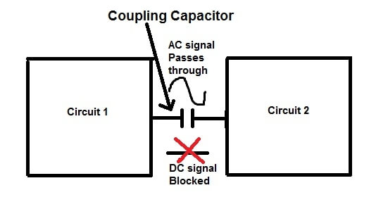
- Capacitive Coupling:Imagine two traces running side by side on a PCB. Whenever a signal passes one trace, an electric field is set up in its surroundings. The electric field might couple over to the adjacent trace and induce voltage in it, hence interference to the signal.
- Inductive Coupling: Current flowing on one trace, changing magnetic field. The magnetic field could couple into adjacent traces, interfering with signals and creating crosstalk.
The closer they are to each other, the traces will have greater interference with one another, since the coupling effect will be stronger.
Also, the amount of crosstalk depends on a number of variables about which you will want to be aware.
Factors Contributing to Crosstalk
Some of the most relevant factors that have the propensity to cause crosstalk in a printed circuit board design include:
- Capacitive Coupling
Electromagnetic coupling happens between traces due to the electric field created by one trace and the voltage on an adjacent trace. This effect is most pronounced in high-speed traces, whereby fast voltage transitions induce noise in adjacent traces.
- Inductive Coupling
Inductive coupling arises because the time-varying magnetic field generated by currents changing in one trace induces spurious currents in nearby traces.
When the circuits have fast-switching signals, the effect becomes very important, for the magnetic field can induce spurious currents in nearby traces and hence distort the signals.
- Trace Proximity
Spacing between traces largely controls crosstalk; this is because close traces increase the possibility of coupling between traces, hence enhancing the effects of crosstalk.
Proper spacing of traces is one of the ways of eliminating interference and keeping the integrity of the signal.
- Signal Characteristics
Yet another critical factor resulting in the existence of crosstalk in a PCB is signal frequency and rise time. Higher frequencies and sharper rise times correspond to more dynamic changes in voltage and current; hence, the influence of the capacitive and inductive couplings between traces is increased.
Without this understanding of the attributes of the signals, there is no way to gain insight into how the reduction of crosstalk in PCB designs can be carried out.
Now let us see how crosstalk is going to degrade a circuit’s operation negatively and ways of reducing its effects.
Impact of Crosstalk on Circuit Behavior
Here’s how crosstalk can impact the circuit behavior:
- Increased Noise
Crosstalk introduces unwanted noise onto victim traces, compromising the integrity of the intended signals. This noise can manifest as random fluctuations or distortions, making it challenging to distinguish between the desired signal and the interference.
In high-speed digital circuits, excessive noise can degrade signal quality and disrupt communication between components.
- Bit Errors
In digital circuits, crosstalk can lead to bit errors by corrupting the transmitted data. When crosstalk interferes with the signals representing binary digits (bits), it can cause misinterpretations or alterations in the data stream.
Bit errors can result in incorrect processing or transmission of information, leading to system malfunctions or data loss.
- Malfunctions
Severe crosstalk can trigger unexpected circuit behavior or component malfunctions. When interference disrupts the normal operation of electronic components, it can lead to system failures, functional errors, or even damage to the hardware.
Malfunctions caused by crosstalk can compromise the reliability and performance of the entire electronic system.
Understanding the detrimental effects of crosstalk underscores the importance of implementing effective mitigation strategies in PCB design.
Now let’s explore practical techniques to minimize crosstalk and optimize circuit performance.
Techniques to Minimize Crosstalk
Here’s how you can minimize crosstalk in your PCB designs:
1.Trace Spacing
Maintaining adequate spacing between signal traces is essential for reducing crosstalk. By increasing the distance between traces, the likelihood of capacitive and inductive coupling decreases, minimizing interference.
Adhering to design guidelines that specify minimum trace spacing helps mitigate crosstalk and ensures signal integrity across the PCB.
2.Ground Planes
Utilizing extensive ground planes in PCB layout acts as a shield against crosstalk and electromagnetic interference (EMI).
Ground planes provide a low-impedance return path for signal currents, reducing the effects of stray electromagnetic fields. Integrating solid ground planes beneath signal traces helps to dissipate noise and enhance the overall performance of the circuit.
3.Differential Pairs
Implementing differential pairs for high-speed signals offers inherent crosstalk mitigation benefits. Differential signaling involves transmitting signals as a pair of equal and opposite voltages, with the receiver detecting the voltage difference between them.
This configuration minimizes susceptibility to external interference, including crosstalk, by effectively canceling out common-mode noise.
4.Routing Techniques
Adopting proper routing techniques plays a crucial role in minimizing crosstalk. Strategies such as avoiding parallel routing of high-speed traces, minimizing trace lengths, and reducing abrupt changes in signal paths help mitigate interference.
By carefully planning the layout and routing of signal traces, designers can minimize crosstalk and optimize signal integrity.
5.Line Impedance Matching:
Implementing line impedance matching techniques helps control signal propagation and minimize reflections that contribute to crosstalk. By adjusting the impedance of transmission lines to match the characteristic impedance of the PCB traces, designers can reduce signal distortion and improve signal fidelity.
Proper termination and impedance control enhance signal integrity and reduce the susceptibility of traces to crosstalk-induced noise.
6.Shielding and Enclosure Design
Implement shielding techniques such as metal enclosures or shielding cans to contain electromagnetic interference and prevent it from affecting adjacent traces.
Proper enclosure design can help minimize the propagation of electromagnetic fields and reduce crosstalk between components.
7.Cross-Hatched Ground Planes
Utilize cross-hatched ground planes instead of solid ground planes to further enhance signal isolation and reduce crosstalk.
The mesh-like structure of cross-hatched ground planes helps to break up electromagnetic fields and mitigate interference between traces.
8.Twisted Pair Cabling
Use twisted pair cabling for signal traces to minimize crosstalk in high-speed and high-frequency applications.
Twisted pair cables consist of two insulated conductors twisted together, which helps to cancel out electromagnetic interference and reduce the impact of crosstalk.
9.Proper Component Placement
Pay attention to the placement of components on the PCB to minimize signal coupling and crosstalk.
Grouping components with similar signal characteristics together and keeping sensitive components away from high-speed signal traces can help reduce interference and improve signal integrity.
10.Impedance Control
Maintain consistent impedance throughout the signal traces by controlling trace width, spacing, and layer stack up. Matching impedance along transmission lines helps to minimize signal reflections and reduce crosstalk-induced noise, improving overall signal quality.
By incorporating these techniques into PCB design practices, engineers can effectively minimize crosstalk and ensure the reliable operation of electronic systems.
Each method contributes to optimizing signal integrity and reducing the risk of interference, ultimately enhancing the performance of the PCB design.
FAQs
How does crosstalk occur in PCBs?
Crosstalk occurs due to capacitive and inductive coupling between traces. Capacitive coupling happens when the electric field from one trace affects the voltage on an adjacent trace, while inductive coupling occurs when changing currents in one trace induce magnetic fields that affect nearby traces.
How can I detect crosstalk in my PCB design?
Crosstalk can be detected through simulation tools that analyze signal integrity and identify areas of potential interference. Additionally, physical testing and signal probing techniques can help identify crosstalk during prototype validation.
What are the common symptoms of crosstalk in PCB circuits?
Common symptoms of crosstalk include signal distortion, unexpected voltage spikes or glitches, data errors in digital circuits, and erratic behavior of electronic components.
Can crosstalk be completely eliminated, or is it always present to some extent in PCB designs?
While it’s challenging to completely eliminate crosstalk, especially in complex PCB designs, it can be effectively minimized through careful layout planning, proper signal routing techniques, and the use of shielding and isolation techniques.
Does crosstalk vary depending on the type of PCB material used?
Yes, the type of PCB material used can influence crosstalk. Materials with higher dielectric constants tend to have stronger capacitive coupling between traces, while materials with higher permeability can affect the inductive coupling between traces.
Conclusion
In conclusion, understanding and addressing crosstalk in PCB design is essential for ensuring the reliability and performance of electronic systems. Crosstalk, caused by capacitive and inductive coupling between adjacent traces, can lead to increased noise, bit errors, and malfunctions in circuits.
However, by implementing practical techniques given in this article, engineers can effectively minimize crosstalk and optimize signal integrity.