


Are you wondering what is chemical etching in PCB manufacturing or what’s the process? You are not getting the idea of how unwanted copper is eliminated from the printed circuit boards to produce the accurate circuit pattern thereon?
Well, you don’t have to worry about that anymore because, in this article, we will elaborate on all the things resulting from chemical etching during PCB manufacturing. By the end, you’ll have a solid grasp of this technique and why it is integral to manufacturing PCBs that are reliable.
OK, let’s get started.
What is Chemical Etching in PCB Manufacturing
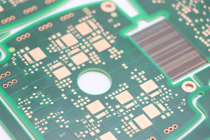
Chemical etching is one of the primary processes for manufacturing PCBs. Unwanted copper is removed by selected chemical reactions with the copper-clad laminate, producing a fine-lined pattern of the desired circuits. It is a crucial step since it reveals the conductive paths, or traces, where electronic components being mounted on the PCB would be interconnected.
Another important role that chemical etching plays is in the ability to create complex circuit designs with repetition and precision. PCBs have found their way around in almost every kind of electronic device, starting from gizmos like smartphones and computers but also including medical equipment and automotive electronics.
Each of these devices comes with a geometry for the respective custom component layout and interconnections with specific electrical pathways that must be designed and implemented precisely using chemical etching.
Moreover, chemical etching allows electronic parts and circuits to be miniaturized, which helps maintain the ongoing trend in developing smaller devices while still incorporating advanced functionality. It steers along some essential industry requirements today—space-saving and efficacy critical.
Now you know the basics of chemical etching in PCB manufacturing, it’s time to learn the process.
The Chemical Etching Process
The chemical etching process in PCB manufacturing involves several key steps to create the intricate circuit patterns necessary for electronic devices.
Here’s the step by step guide that will help you:
1.Design and Photoresist Application:
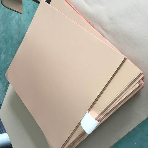
In this process, the PCB is to be designed by laying out the plan using CAD software or computer-aided design. This layout defines the placement of components and the electrical connections (traces).
A layer of photoresist material is then applied onto the copper-clad laminate. This photoresist acts as a protective mask that will define where the copper will be removed during etching.
2.Ultraviolet (UV) Light Exposure:
A photomask, which contains the circuit pattern, is placed over the photoresist-coated PCB.
The PCB is exposed to UV light. The areas of the photoresist not protected by the opaque parts of the photomask will undergo a chemical change, becoming either more soluble or less soluble (depending on the type of resist).
3.Development:
The PCB is activated and developed after curing. Activation refers to the process of washing the PCB with an activator solution in preparation for exposure. After activation, the PCB is developed through a washing process using a developer solution, which essentially dissolves away the unexposed or weakly tacked photoresist.
Therefore, the developed PCB now displays regions of copper where the circuit traces and pads are to be made.
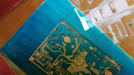
4.Etching:
The circuit board is then placed into a solution known as an etchant, often a type of acid, such as ferric chloride or ammonium persulfate.
The Etchant attacks the copper selectively, meaning it only dissolves the areas of copper that the remaining photoresist does not protect. This process continues until all unwanted copper is completely dissolved, leaving behind only a circuit decorated on the PCB.
5.Stripping:
The remaining photoresist coat from the PCB is stripped off.
Stripping is generally a process entailing chemical solutions and solvents that dissolve and remove photoresist to leave a clean copper-free surface of all tracings and pads.
6.Inspection and Cleaning:
Here, determine whether the main objective of the etching process is to leave only the desired circuit pattern without any flaws or whether the etching is appropriately carried out.
The board inspection cleans no residues remaining from both the etching and stripping processes.
Chemical Etching Solutions
Chemical etching solutions are fundamental to the PCB manufacturing process, as they enable the precise removal of unwanted copper from circuit boards.
The etchant solution is based on ferric chloride or cupric chloride itself, both reacting from a chemical mechanism, enabling the contact-exposed copper to gradually dissolve.
Some of the most widely utilized etchants include ferric chloride, which is very effective in this removal. It acts by causing the oxidation of copper metal. This oxidized copper metal has taken a soluble form in the copper chloride state, leaving it to be washed away.
Cupric chloride, on the other hand, is preferable in some applications due to its higher metal system etch rate and reduced metal system corrosion rate.
The correct choice of the etching solution depends on the base material of the PCB and the thickness of the copper layer. The solutions differ in their canopy of application; some at varied temperatures, some in different concentrations, hence some etch at a varied speed; in others, there is uneven etching.
A proper understanding of these solutions is required by a PCB manufacturer to do an accurate and uniform production of the circuit board.
Factors Affecting Etching Rate and Uniformity
Achieving optimal etching results in PCB manufacturing relies on several key factors that influence both the rate of etching and the uniformity of the process.
1. Etching Solution Concentration and Temperature
The concentration of the etching solution, such as ferric chloride or cupric chloride, directly affects how quickly it can dissolve copper. Everyone must regulate the etching solution within optimum control under suitable conditions to avoid either over-etching or undercutting valuable traces in the copper.
Warm solutions generally etch rapidly compared to cool ones, particularly considering the temperatures. This calling for constant temperatures is a crucial factor during such exercises to produce commendable and consistent results.
2. Agitation of the Etching Bath
Agitation of the etching bath ensures that the etchant is even on the surface of the PCB, whereby it helps remove dissolved copper ions from the surface and, at the same time, replaces fresh etchant.
That way, there will be a uniformity in etch rate throughout the board. If this is not agitated adequately, traces will vary in thickness and integrity, leading to non-uniform etching.
3. Board Design Complexity and Feature Size
The complexity of the PCB design and the size of its features directly impact the etching process. Some accommodation may, therefore, have to be made in terms of etching time or solution concentration to achieve uniformity in the feature sizes, since more extensive features may etch at a different rate than their smaller counterparts.
4. Achieving Uniform Etch Rate
The etch rate should provide strength by assurance that all of the desired copper traces will be etched to the correct depth and contour. If this rate is not reasonable, there is a chance that certain positions might be over-etched and have thin or broken traces or under-etched and have copper where it shouldn’t be on the board.
Such uniformity over the etched workpiece can be achieved only by care in the control of the parameters of the etching solution, its methods of agitation, and the consideration of the associated design complexities in the actual manufacturing of electronic products.
Now let’s discuss the advantages and disadvantages of chemical etching in detail.
Advantages and Disadvantages of Chemical Etching
There are both advantages and disadvantages of chemical etching that you must know:
Advantages
- Simple and Inexpensive for Simple PCB Designs: Chemical etching is easy and inexpensive; therefore, it is perfect for simple PCB designs. This process is not critical about the equipment, so it is not expensive.
- Proven Traceable Dependable Results:This technique has been efficiently proven for some time and has shown its worth in PCB manufacturing. No matter what, with this technique, manufacturers can produce a consistent creation of circuit patterns that could yield correct and accurate results.
- Versatile for Copper Thickness: Be it the thick or thin layers of copper, chemical etching can ideally handle all thickness gradients. It is then versatile for very different application needs or design requirements.
Disadvantages
- Environmental Issue with Chemicals Disposal: Disposing of the chemicals used in etching, like ferric chloride, requires careful handling due to environmental hazards. Proper disposal adds complexity and cost.
- Problems in Complex Designs: Complex PCB designs are prone to uneven etching or undercutting of copper traces. To achieve a uniform result, you would have to have extreme control over this etching process.
- Limitations on Very Fine Features: For dense, high-layer-count PCBs that require microvias or excellent features, chemical etching cannot provide the necessary type of precision. For this level of precision work, you must use laser ablation.
Understanding these pros and cons helps PCB manufacturers choose the best manufacturing approach based on their specific needs, balancing cost-efficiency, technical demands, and environmental considerations.
Alternative Methods
In addition to chemical etching, several alternative methods offer distinct advantages in PCB manufacturing, catering to different design requirements and precision needs:
- Laser Ablation:
The primary application of laser ablation involves processes working on focused laser beams, making way for a selectively removed material from the substrate of the PCB. It’s ideal for creating patterns defined as accurate and precise, composed of microvias and small features that chemical etching cannot perfect.
This process will minimize scrap material and provide a very high degree of accuracy that is needed for high-density interconnections.
- Plasma Etching:
The etching is performed using ionized gas, plasma. The excellent control of the depth of etch and profile allows for complex geometries and a uniformity of results to be obtained across the board. Different materials can be handled in plasma etching that will go well for the fine-line PCBs.
- Dry Etching Processes:
While in dry etching, RIE, and IBE, methods of chemical reaction or ion bombardment are used on the PCB to etch material from the substrate, chemical methods in such an etching are very accurate, with detailed patterns and very minimum undercutting.
Such etching processes are ideal in modern PCB making when there is the need to get sophisticated geometries in the critical feature’s dimensions and depths.
Many of these methods are selected by the PCB manufacturers depending on the specific production requirements and expected outcomes in terms of quality, efficiency, and technological advancement.
Conclusion
In conclusion, chemical etching is a cornerstone of PCB manufacturing and vital to creating precise circuits—essential for a modern electronic device. The feature makes it both simple and cost-effective for simple designs and flexible across various copper thickness applications.
Nevertheless, laser cutting also has disadvantages, including environmental concerns and difficulty working with intricate designs or even excellent features. So keep everything in mind before making your decision.