


Vias Overview
Imagine a city built on layers, but without ramps or bridges between them. That’s kind of what a circuit board would be like without vias! Vias are like tiny tunnels drilled through the board that connect different layers with copper. They allow electricity to flow between these layers, making your circuit board function properly.
What are Vias?
Vias are holes on the circuit board that connect the lines between various layers, transforming the circuit board from a flat structure to a three-dimensional one. Production of via holes involves plating a layer of metal on the cylindrical surface of the via wall, which connects the copper foils of the middle layers. The upper and lower sides of the via holes are made into pad shapes for direct line connections.
Why are Vias Important?
It’s difficult to imagine single-layer circuits without needing to cross over traces. Two-layer or double-layer circuits must be connected through vias. These vias use the copper on the inner wall of the hole to connect the circuit copper wires on the upper and lower layers. In some cases, single-sided PCBs require vias to change layers for proper routing.
Types of Vias
Vias are generally divided into three categories: through-hole vias (THVs), blind vias, and buried vias.
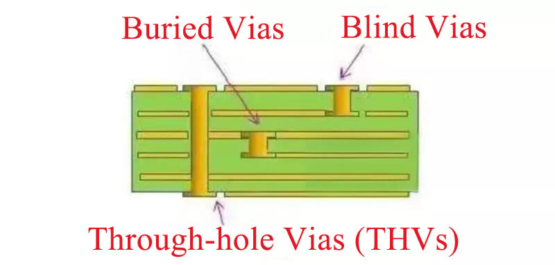
Through-hole Vias (THVs)
The most common and reliable via type, THVs are created by drilling a hole through the entire PCB and filling it with conductive material like copper. They connect all layers of the board.
Blind Vias
Similar to THVs, blind vias are partially drilled holes that connect an outer layer to an inner layer without going all the way through the board. Offering a space-saving advantage, they are ideal for multi-layer PCBs with limited space.
Buried Vias
Completely hidden within the PCB, buried vias reside entirely between internal copper layers. They provide the highest density and best signal integrity but are the most expensive and challenging to manufacture due to the drilling depth required.
Microvias
For situations demanding even tighter spacing, microvias come into play. These laser-drilled vias are incredibly small, typically less than 6 mils, and connect only two adjacent layers. They offer exceptional space savings and design flexibility but are more expensive to fabricate due to the precise drilling process.
Via-in-pad (VIP)
Unique vias located within a surface mount component pad, VIPs can be standard THVs or microvias. They offer the advantage of connecting a component directly to an inner layer without requiring additional routing space. However, careful design considerations are needed to prevent solder from flowing down the via hole during assembly.
Their Role in PCBs
- Signal Routing: Most circuit boards utilize through-hole vias for signal routing on a grid. Denser boards might incorporate blind or buried vias, while very dense ones rely on microvias.
- Escape Routing: Larger surface mount components typically use through-hole vias to connect to outer layers. In some cases, blind vias or microvias might be used.
- Power Routing: Vias used for power and ground nets need to handle higher currents, so larger through-hole vias are usually preferred.
- Stitching Vias: These vias provide multiple connections to a plane, typically through-hole or blind vias. They can be used for EMI protection by connecting a sensitive circuit area to a ground plane.
- Thermal Vias: Here, vias act as heat conductors, transferring heat from a component to an internal plane layer. These are often larger through-hole or blind vias, frequently placed within the component pads themselves.
Impact of Vias in PCB Performance
Signal Integrity
- Disruption and Impedance Mismatch: At high frequencies, vias act like interruptions in the signal path. This disrupts the intended impedance of the trace, causing signal reflections and introducing timing errors (jitter).
- Parasitic Effects: Vias introduce tiny amounts of unwanted capacitance and inductance. This can slow down the signal rise time and create unwanted resonances and distortions. The severity of these impacts depends on the signal frequency and the via design.
Power Distribution
- Increased Inductance: The main concern with vias in power distribution is their parasitic inductance. This inductance can impede the flow of current, particularly for high-current applications.
- Power Plane Disruption: Vias create holes in power planes, which can disrupt the flow of current across the plane. This can lead to uneven current distribution and localized voltage drops.
Other Design Considerations
Impedance Control
Vias can disrupt the intended trace impedance due to their change in geometry. This can cause reflections and signal integrity issues, especially at high frequencies. To mitigate this, strategically place vias to avoid disrupting the trace impedance. Additionally, avoid sharp bends or stubs (short trace extensions) around vias.
Crosstalk: Vias in close proximity to signal traces can introduce crosstalk. This happens because the changing current through the via can couple some energy into nearby traces, causing unwanted signal interference. To minimize crosstalk, maintain sufficient spacing between vias and signal traces. Refer to your PCB design rules for recommended spacing guidelines.
Noise: Vias themselves can contribute to noise by acting as small antennas, especially at high frequencies. The rapid changes in current through the via can radiate electromagnetic interference (EMI). To minimize noise issues, utilize grounding vias strategically to provide a good return path for current and reduce unwanted inductance loops. This is especially important for high-frequency signals and power delivery.
Thermal Management
Vias can play a role in thermal management by providing a path for heat transfer between layers. However, they can also introduce thermal resistance. Here are some considerations:
- Larger vias: Use larger diameter vias whenever possible for improved heat dissipation.
- Thermal vias: For components generating significant heat, consider using larger, thermal vias filled with thermally conductive materials to improve heat dissipation between layers. These are often placed within the component pads themselves.
Best Practices for Using Vias
Via Selection
- Through-hole vias (THVs): Suitable for low-frequency applications and power delivery where space is less critical.
- Blind vias: Offer better density and signal integrity compared to through-hole vias but are more complex to manufacture.
- Buried vias: Provide the highest density and best signal integrity but are the most expensive and challenging to manufacture.
- Microvias: Ideal for high-density boards but require precise manufacturing and are more susceptible to defects.
General Via Size Best Practices
- Minimize via count: Use the fewest vias possible to achieve the desired routing. This reduces parasitic effects and improves overall signal integrity.
- Aspect ratio: Aim for a via aspect ratio (height to diameter) as close to 1:1 as possible. This minimizes inductance and improves signal integrity. However, taller vias may be necessary for proper plating in some cases.
- Via diameter: Use the largest via diameter possible based on design constraints. This reduces via inductance and improves current carrying capacity.
Via Layout Best Practices
- Via minimization in critical areas: For high-speed signals or noise-sensitive components, prioritize minimizing vias in those areas.
- Staggered vias vs. stacked vias: Use staggered vias instead of stacked vias whenever possible. Stacked vias require filled and plated vias, increasing cost and complexity.
- Via placement for impedance control: Strategically place vias to avoid disrupting the intended trace impedance. Avoid sharp bends or stubs (short trace extensions) around vias.
- Via spacing: Maintain sufficient spacing between vias and signal traces to minimize crosstalk. Refer to your PCB design rules for recommended spacing guidelines.
- Grounding vias: Utilize grounding vias strategically to provide a good return path for current and reduce unwanted inductance loops. This is especially important for high-frequency signals and power delivery.
- Thermal vias: For components generating significant heat, consider using larger, thermal vias filled with thermally conductive materials to improve heat dissipation between layers.
Conclusion
Vias are essential components in multilayer PCBs, enabling connections between different layers and facilitating complex circuit designs. By understanding the different types of vias, their impact on performance, and best practices for using them, you can optimize your PCB design for functionality, signal integrity, and thermal management.