


Wondering what are pads in a PCB? Well, pads are the circuit board essentials, but they can be tricky to understand. They help connect all of the components, but it can sometimes be really hard to know which type to use or how to design them.
This article will help you grasp everything about PCB pads in simple terms. We will show how different types are designed and some common mistakes to avoid.
So, let’s get started.
What is a PCB Pad
PCB pads are small, flat areas on a printed circuit board where electronic components are attached. They are essential for making connections between components and the copper traces on the PCB.
A PCB pad generally is a conductive surface, usually of copper material, to which some components are soldered. These pads are in varied shapes and sizes for sitting different components.
They are designed to provide the PCB with strong, reliable solder joints; this is important for correct functioning.
Function of PCB Pads in Connecting Components
PCB pads have three main functions:
- Electrical Interconnection: Pads provide a conductive surface for soldering components, creating a stable electrical link between the component leads and the PCB’s copper traces.
- Mechanical Support:Pads hold the components in place on the board, ensuring they stay securely attached.
- Heat Dissipation: Pads spread the heat emanated by components so that no heating occurs at one point and damages the component.
The pads ensure proper connections, which keep the entire electronic circuit working in the right way.
Now let’s discuss the different types of PCB pads in detail.
Types of PCB Pads
PCB pads come in two main types: through-hole pads and surface mount pads.
Each type has specific features and is used for different applications.
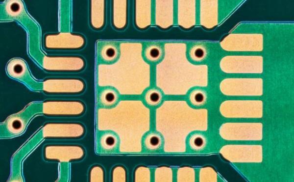
Through-Hole Pads
Through-hole pads are there for mounting component leads that pass through holes in the PCB. These may be larger and usually round or square.
- Purpose and Function:
Through-hole pads have high mechanical strength due to the fact that the component leads pass through the board and are soldered on the reverse side of it. This makes them quite suitable for any components that undergo physical stress.
- Common Shapes and Sizes:
Standard through-hole pads are either circular or square but can be any other shape, depending on the application at hand. Their sizes vary with the intent that they more or less match those of the lead component.
What’s really important is the internal diameter and clearance for proper holding power and reliability.
- Importance of Hole Diameter and Pad Clearance:
The diameter of the hole must be equal to that of the lead size of your component to get a good fit. While pad clearance ensures there’s enough space around the hole to avoid short circuits and ensure a strong solder joint.
Surface Mount Pads
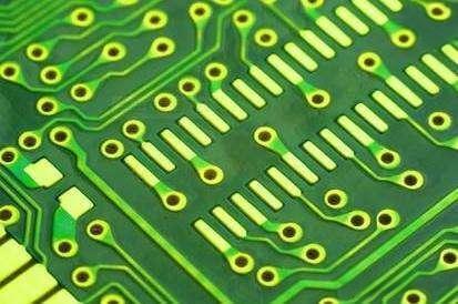
Surface mount pads are meant for components that are directly soldered onto the surface of the PCB. They are mainly made much smaller and may come in several shapes, such as square, rectangular, and oval.
- Purpose and Function:
Surface mount pads are more compact and resourceful ways through which PCBs can be designed. They go with the components that don’t have a lead passing through the board, but find their application in high-density applications.
- Common Shapes and Sizes:
Surface-mount pads may be square, rectangular, or oval, though their dimensions are determined by the particular component they serve. The shapes and sizes are designed to match with the component leads or terminals.
- Land Patterns and Stencil Openings:
Land patterns are the arrangement of surface mount pads on the PCB. Stencil openings are used in the soldering process to apply solder paste accurately onto the pads, ensuring proper component placement and soldering.
Figuring out these different types of pads on a PCB and their functionality can greatly help in deciding what to make while designing and assembling printed circuit boards.
Pad Design Considerations
Designing PCB pads requires careful consideration of several factors to ensure reliable and efficient performance.
- Importance of Pad Size and Shape
The size of a pad is crucial for creating a strong solder joint. If a pad is too small, it may not provide enough area for a good connection, leading to potential failures. Conversely, if it’s too large, it might cause solder bridging between pads.
The shape of the pad affects how well the component fits and how easy it is to solder. Common shapes include round, square, rectangular, and oval. The shape should match the component lead or terminal to ensure a secure fit and proper solder flow.
- Copper Thickness and Plating
The thickness of the copper layer on the PCB impacts the pad’s ability to carry current and dissipate heat. Thicker copper layers provide better current-carrying capacity and heat dissipation but may increase the cost and complexity of the PCB.
Plating the pads with materials like gold, silver, or tin helps protect the copper from oxidation and improves solderability. The choice of plating material can affect the pad’s durability and performance.
- Pad Clearance and Spacing
Clearance refers to the space around the pad. Adequate clearance is necessary to prevent short circuits and ensure that the solder doesn’t bridge to adjacent pads or traces. Proper clearance also allows for better heat dissipation.
Spacing between pads must be sufficient to avoid short circuits and accommodate the component size. Tight spacing can lead to solder bridges and assembly issues, while excessive spacing can waste valuable PCB real estate.
- Thermal Consideration
Pads must be designed to handle the thermal loads of the components they support. Proper thermal management ensures that heat is efficiently dissipated, preventing overheating and damage to both the pad and the component.
For through-hole pads, thermal relief connections (small, radial copper traces) are used to connect the pad to the copper plane. This helps in soldering by balancing the heat distribution and preventing thermal stress on the pad.
By considering these factors during the design phase, you can ensure that your PCB pads are reliable, durable, and effective in their roles. Proper pad design is essential for the overall performance and longevity of your printed circuit board.
Pad Soldering Process
Soldering pads is a key step in making sure your PCB works well. Here’s a simple guide to the soldering process:
1.Preparation
First of all, you will have to do some preparation work:
- Clean the Pads: Make sure the pads are clean. Use a flux cleaner or isopropyl alcohol to remove any dirt or oxidation.
- Apply Flux: Put flux on the pads. This helps the solder stick better.
2.Soldering Methods
There are two main ways to solder pads: hand soldering and reflow soldering.
Hand Soldering:
- Heat the Pad: Use a soldering iron to heat the pad and the component lead at the same time. The temperature should be around 350°C (662°F).
- Apply Solder: Touch the solder wire to the heated pad and lead. The solder will melt and flow around them. Remove the soldering iron and let the joint cool.
- Inspect the Joint: Check the solder joint. It should be smooth and shiny. If it looks rough or cracked, it needs to be redone.
Reflow Soldering:
- Apply Solder Paste: Use a stencil to put solder paste on the pads. The paste has tiny solder particles in it.
- Place Components: Put the components onto the solder paste-covered pads. The paste will hold them in place.
- Reflow Oven: Put the PCB through a reflow oven. The heat will melt the solder paste and form the joints. Then, the PCB is cooled down slowly.
- Inspect the Joints: After reflow soldering, check the joints to make sure they are good. You can do this by looking at them or using special inspection tools.
By following these steps, you can make strong, reliable solder joints on your PCB pads.
Common PCB Pad Design Mistakes and How to Avoid Them?
Designing PCB pads can be tricky, and mistakes can lead to problems with your circuit board. Here are some common mistakes and how to avoid them:
1.Incorrect Pad Size
Pads that are too small or too large can cause issues with soldering and component placement.
Ensure pads are the correct size for the components. Use manufacturer specifications and design guidelines to determine the right size.
2.Inadequate Pad Clearance
Insufficient clearance around pads can lead to short circuits and solder bridges.
Maintain proper clearance between pads and nearby traces or components. Follow industry standards for pad clearance to avoid electrical issues.
3.Poor Pad Plating
Using the wrong plating material or having poor-quality plating can result in unreliable solder joints.
Choose the right plating material, such as gold, silver, or tin, based on your application. Ensure the plating process is done correctly to prevent oxidation and improve solderability.
4.Improper Pad Shape
Using the wrong pad shape can make it difficult to solder components properly.
Select the appropriate pad shape for each component. Common shapes include round, square, rectangular, and oval. Match the pad shape to the component lead or terminal.
5.Incorrect Pad Spacing
Pads that are too close together can cause solder bridges, while pads that are too far apart can lead to weak connections.
Ensure proper spacing between pads to prevent solder bridges and ensure strong solder joints. Use design software to check pad spacing and make adjustments as needed.
Conclusion
Understanding PCB pads is important for designing reliable circuit boards. Pads connect components, support them mechanically, and help with heat dissipation. There are two main types of pads: through-hole and surface mount. Knowing when to use each type is key.