


Are you struggling to understand the function of the solder mask layer in PCB design? Or you are wondering what is the importance of the solder mask layer in PCBs? If yes, don’t worry at all as this guide is here to help you.
We will guide you through its functions, types, application processes, and standard defects so that the designs are professional and reliable.
By the end, you’ll know enough to fix your solder mask issues so you can make high-quality PCB.
So, let us begin.
Understanding Solder Mask Layer in PCBs
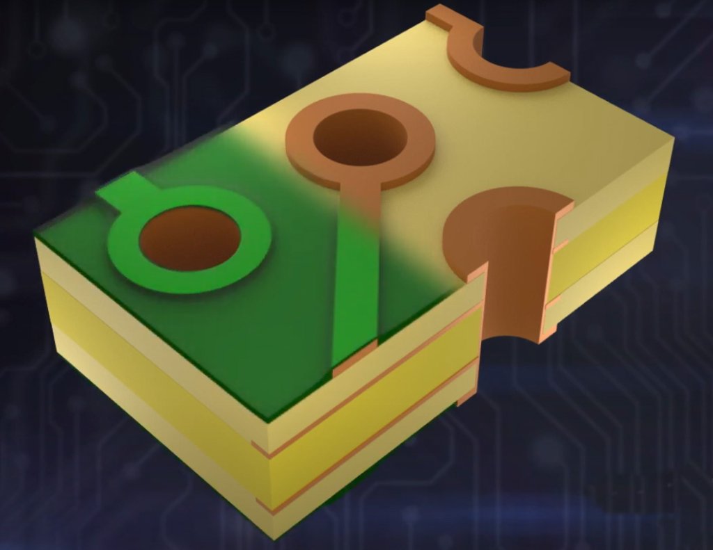
One of the most significant layers involved in PCB design is the solder mask layer. It is the application of a protective coating on the PCB, covering the copper traces and pads so that no unwanted shorts between components occur during the soldering process due to the solder.
Essentially, it is a non-conducting coating that acts as a guard for the integrity and functionality of your PCB.
Here’s why the solder mask layer is really important:
- Ensures Proper Electrical Isolation
The solder mask layer assures good electrical isolation between conductive elements on the PCB. Such isolation is crucial for the correct functionality of a board, avoiding electrical shorts that may malfunction or even damage it.
- Protects Copper Traces
The copper traces on the PCB are sources of potential corrosion and are very sensitive to detrimental influences of the environment, specifically moisture, and contaminants. The solder mask layer helps protect the copper tracks from corrosion, therefore extending the life of the printed circuit board.
- Enhances Visual Appeal and Professionalism
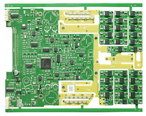
A good solder mask layer in place gives a PCB a nice, professional look. The layer completely covers the copper traces and pads, exposing only the necessary areas. This not only provides an aesthetically pleasing appearance but also underlines the visibility of different sections and components when going through assembly and inspection processes.
Now let’s discuss the functions of solder mask in PCB design in detail.
Functions of Solder Mask in PCB Design
The solder mask layer performs several critical functions in PCB design, ensuring the board’s performance and longevity.
- Solder Damming
One of the significant roles of the solder mask layer is to do the job of solder damming. A primary sufficient task is to permit the flow of solder everywhere except in between specific conductive areas while soldering.
It ensures that solder sticks only where necessary and doesn’t lead to problems such as short circuits.
- Electrical Insulation
Another essential function of the solder mask is electrical insulation. The non-conductive barrier insulates the traces and pads from each other and stops electrical shorts from forming, thereby maintaining an electrical pathway’s integrity.
This insulation is critical to make sure the overall PCB performs right, particularly with designs of high density and numerous traces that are too close to each other.
- Mechanical Protection
The solder mask layer provides mechanical protection to the copper traces of the PCB. Physical abuse and abrasion to these traces are protected during handling, assembly, and operation.
These protective layers prevent mechanical wear that may lead to circuit failure.
- Marking and Identification
It can also be used for marking and identification purposes besides protection. The mask on the solder allows color-coded marking, the addition of logos, and other identifiers onto the PCB.
This thus facilitates the identification of the different segments of the board, which can help a layout for the best use of the assemble and hence implementation.
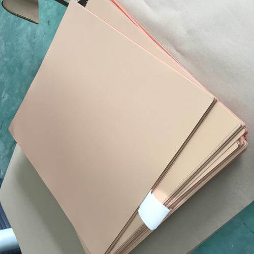
Types of Solder Mask Materials
Choosing the right solder mask material is essential for ensuring the durability and functionality of your PCB.
Here are the main types of solder mask materials commonly used in PCB manufacturing:
1.Epoxides
A majority of the materials for solder masks in a PCB design are epoxides; they demonstrate excellent adhesion to the board, good chemical resistance, and are affordable.
This makes epoxides all-round application materials, granting solutions in most situations regarding protection and durability, besides being cost-effective.
2.Polyimides
One of the high-performance solder mask materials is polyimide. These materials have very good thermal and chemical resistance, hence considered for most critical applications where the PCB needs to endure demanding conditions.
Polyimides, to a greater extent, find numerous applications in aerospace, automotive, and high-temperature industrial applications due to this superior performance characteristic exposed.
3.Acrylates
Acrylates are known for their fast processing times and good solderability. These properties make them an attractive choice for manufacturing environments that require quick turnaround times.
However, acrylates typically have lower chemical resistance compared to epoxides, which may limit their use in applications where chemical exposure is a concern.
With an understanding of the different types of solder mask materials, you will be able to pick the best-performing material in a given PCB design, providing an awareness of performance and considering both durability and cost.
Now you know the basics of solder mask layer in PCBs, it’s time to learn the process in detail.
Applying Solder Mask During PCB Fabrication
Applying the solder mask is a critical step in PCB fabrication, involving several stages to ensure a reliable and defect-free protective layer.
Here’s a detailed look at the process:
Step #1: Panel Preparation
The first step in this process is cleaning and making ready the PCB panel, where surface preparation is done.
This makes sure the surface is free of any contaminations, which gives way to the application of the solder mask. Proper cleaning will gain good solder mask adhesion onto copper traces and pads.
Step #2: Solder Mask Application
Next is the application of a solder mask. Generally, this is applied using liquid solder mask material, which is again applied by screen printing or stencil printing.
Screen printing is done mainly for regular applications and leans toward stencil printing for more complicated or unique applications. A soldier mask is applied to evenly coat the PCB board.
Step #3: Exposure and Development
Following the application of the solder by using a solder mask, the desired pattern is exposed to ultraviolet light, referred to as the exposure. With the aid of a photomask, the areas where the solder mask is supposed to remain, and the areas from which it should be washed away are defined.
Following the exposing of the board to ultraviolet, development follows, in which the non-exposed solder mask is being washed away, ensuring that only places specified receive the protective layer.
Step #4: Curing
The solder mask layer is permanently hardened by curing, usually through partial drying/baking. This step will ensure that the solder mask has been fully set; it is now ready and durable for protecting the copper traces during soldering and across the life of the PCB.
Step #5: Inspection
Inspection is the last step in this list. The solder mask layer herein will be examined for various defects, say, poor cover-up, pinholes, misalignment, and the most negligible thickness.
Such an approach can be either subjective through human examination with magnification or implemented objectively in the form of an Automated Optical Inspection (AOI).
Detecting and rectifying any flaws during this stage is important to reduce issues while the PCB operates.
When perfected, these steps assure top-notch and dependable application of a quality solder mask on your printed circuit boards, increasing their performance and durability.
Solder Mask Defects and Inspection
Even with careful application, defects in the solder mask layer can occur that will significantly affect the functionality and reliability of the PCB.
Understanding such defects and their inspection would, in turn, serve to maintain high-quality production in PCBs.
Common Solder Mask Defects
- Pinholes: These are minor fractures within the solder mask that allow the underlying copper to be exposed. Exposed areas could potentially create and offer paths for current and, later on, destroy the electrical integrity of the PCB.
- Solder Bridges:Solder bridges are unintended solder connections between components caused by unsealed portions of solder mask. These may cause a short, malfunction, or non-function within the PCB. They are defective material usage and defective.
- Misalignment: This occurs when the placing of the solder mask, relative to the copper traces, is incorrect. This may lead to some areas not being fully protected and copper possibly showing. As a result, making the PCB prone to shorts and corrosion.
- Insufficient Coverage: It is the incompletely covered region of copper traces by the solder mask. These exposed copper areas are easily corroded and cause electrical shorts again, further eroding the lifespan and reliability of that PCB.
Importance of Solder Mask Inspection
Solder mask needs to be defect-free for the excellent quality and overall performance of the PCB.
This is why inspection is so important:
- Checking the electrical functionality:Electrical testing is going to help check for impending shorts caused by defects such as pinholes or even solder bridges. By testing for electrical paths, manufacturers can pick up electrical points that require troubleshooting to repair the culprits, hence preventing the failure of the PCB.
- Visual Inspection: Detected visible defects include but are not limited to pinholes, misregistration, and insufficient coverage. The layer of solder mask is put under magnification at the time of manual check so that each visible defect is taken into consideration and then corrected.
- Automated Optical Inspection:Automated Optical Inspection is the one essential used in producing high-level PCBs. AOI systems use sophisticated imaging technology to scan the PCB carefully for any possible defects. This is a fast, effective way to serve homogeneous quality across significant production runs.
So, by conducting rigorous defect inspection of the solder mask layer, the manufacturers can guarantee the quality and ascertain that their PCBs are reliable and durable enough to avoid future problems that would be destructive to their investment.
Design Considerations for Solder Mask
Here are some additional design consideration for solder mask that will help you:
1.Minimum Solder Mask Clearances
Proper spacing between traces and pads is quite crucial to their necessary soldering flow and appropriate component attachment. This offers adequate clearances for avoiding solder bridging and shorts, allowing clean and accurate soldering.
2.Solder Mask Dams
A solder mask dam, on the other hand, is an isolation boundary constructed around the pads to control the flow of the solder during assembly.
Therefore, these dams avoid the spreading of solder in other places than the ones intended or towards delicate areas, assuring precision and reliability of the solder joints.
3.Vias and Exposed Pads
Proper application of via tenting and exposed pad dimensions plays a critical role in the appropriate solderability of exposed vias.
Vias tented with a solder mask will help to shield the vias from contamination and accidental solder bridging, and exposed pads are designed for maximum available solder coverage for the best reliability in connection.
4.Design for Manufacturability (DFM)
Now, designers need to keep in mind such limitations in the process of applying solder masks to avoid designing features that turn into bothersome trouble later.
Designers must consider the precision of mask application, not designing features that are very fine and too complex in features, which may cause misalignment and partial coverage.
Conclusion
Understanding the solder mask layer is key to making high-quality and reliable PCBs. This guide has covered its functions, types, application steps, common defects, and design tips.
With this knowledge, you can avoid issues like solder shorts and corrosion while also improving the look and durability of your boards.