


PCB Via Definition
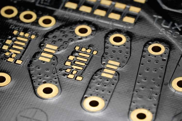
PCB via, also called a metallized hole, is a common hole drilled through a double-sided or multilayer printed circuit board to connect printed wires between layers. In terms of technology, a layer of metal is plated onto the cylindrical walls of the via hole using chemical deposition to connect the copper foils. The top and bottom surfaces of the via are shaped into circular pads. The main parameters of a via include the hole’s outer diameter and drilling size.
FAQs
PTHs and vias are holes used in PCBs for conducting electricity. PTHs pass through the entire board and connect different layers. In contrast, vias are used to connect different parts or components on the same PCB layer.
*Source:https://camptechii.com
The most common via size is 10 mil, which is 7 mil after plating, but via size typically depends on the thickness of the board and is considered an aspect ratio equation. Micro vias, both laser drilled and mechanically drilled 4 mil holes, are related to the thickness of the boards.
*Source:https://www.cirexx.com
Not all PCB vias need solder mask opening, it all depends on your PCB needs. For better thermal dissipation of your PCB, you can design solder mask openings for the PCB vias. Especially for power supply PCBs that flow large currents, solder mask opening for thermal dissipation is common.
*Source:https://www.pcbonline.com
Vias are crucial for designing complex and compact electronic circuits where traditional surface routing might be impractical. In addition to their role in electrical connectivity, vias also impact the signal integrity of the PCB, especially in high-speed designs.
*Source:https://www.sierraassembly.com
Vias can be circular or non-circular, and their diameter can range from a few mils to several hundred mils. The placement of vias is also critical in PCB design. Vias are typically placed in areas where there are no critical components or traces, as they can interfere with the signal or cause electrical noise.
*Source:https://jlcpcb.com
Zero Defect
Quick-turn service
PCBA Manufacture
Learn how Keep Best can turn your designs into products.