


Are you wondering what silkscreen on a PCB is? Have you ever had issues with bad and unreadable marks on the board when working with a PCB? It’s a common problem and may cause confusion, leading to some expensive errors during assembly processes. The good news is, proper understanding of PCB silkscreen is all you need.
So in this article, you will be provided with a step-by-step guide on what silkscreen is, why it is important, and how it is applied. At the end, you will feel more confident reading and designing PCBs with clear and organized labels.
So, let’s get started.
What is Silkscreen on a PCB
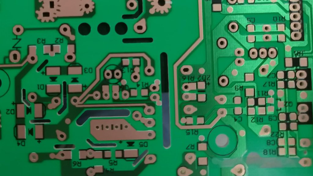
Silkscreen on a PCB refers to the layer of ink printed on the board’s surface, used primarily to label and identify components, test points, and other critical information. This layer, most of the time, exists in both the top and bottom parts of the board and can be used by engineers, technicians, and manufacturers in assembly and testing.
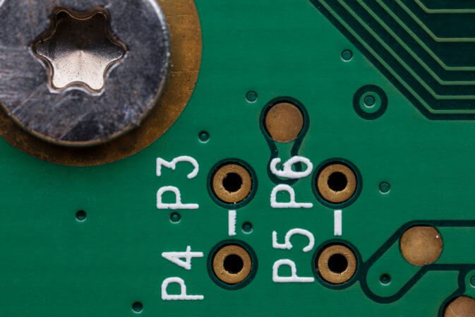
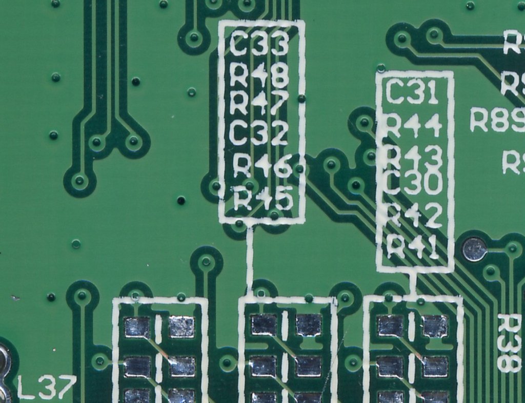
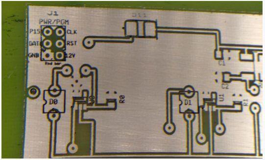
The silkscreen layer is normally used for including text, symbols, and other indications of component locations, reference designators (e.g., R1 for a resistor or C1 for a capacitor), and sometimes even revision numbers.
A PCB lacking these last two elements would hardly be plausible for assembly and debugging.
Relationship Between Silkscreen and Solder Mask
The two dissimilar layers are the solder mask and silkscreen; they are very distinct from each other but work in harmony within a PCB. The copper traces are coated with a solder mask to protect them from a potential short circuit.
A silkscreen layer is put on top of a solder mask layer for labeling or guidance purposes. Proper alignment of these layers is very necessary to avert it from blocking pertinent information or generating design flaws.
Silkscreen Process
The silkscreen process consists of several steps that ensure an accurate and durable label on the surface of the PCB:
- Surface Preparation:The PCB is clean and ready for printing in order to bring on the ink in the right way.
- Applying the Silkscreen:Some of the ways of applying silkscreen include, for example
- Manual Screen Printing:That’s the traditional method by which ink is pushed through a screen.
- Liquid Photo Imaging (LPI):A more precise Liquid Photo Imaging process utilizing photosensitive ink and UV light.
- Direct Legend Printing (DLP):A direct digital process in which a printer lays down ink directly on the board.
- Exposure and Development:The LPI board is exposed to ultraviolet light to dry, followed by wiping down the non-exposed areas.
- Drying and Curing:Ink is dried and cured so it dries hard enough to withstand the life of the board.
Design Guidelines for Silkscreen:
The text should be an acceptable size such that it is easy to read but not too big to fit inside the printable area. The recommended text height ranges from 0.8 mm to 1.0 mm. Line width and thickness should be optimized to prevent smudging or fading while maintaining clarity.
The proper size means that while it needs to be large enough to avoid mistakes when soldering and small enough to fit in the printable area, in general, it should be sufficiently big so that it can be read.
Always ensure the text and symbols do not overlap any pad, via, or trace.
Legend Placement and Content:
- What Information is Placed:The silk screen probably will contain reference designators (eg. R1 for resistors or U1 for ICs), polarity markers, component outlines, and version numbers. It should be confirmed that all critical data are very visible; for example, component labels as well as test points.
- Where Information is Placed:Shields should be placed in locations where the assembly and testing processes clearly allow them to be read. Do not orient silkscreen marking very close to, or unwittingly on top of, solder pads and components.
Color Selection:
The most common colors for silkscreen are white, yellow, and black. White is the most standard choice in color, as it offers the best contrast against most of the solder mask colors that are in use, like green and blue.
Yellow or black can also be used according to the board’s overall color scheme. The best contrast between silkscreen and solder mask significantly enhances readability, especially in poor lighting.
Silkscreen Thickness and Material:
- Thickness:The thickness of the silkscreen layer is crucial. A typical range is between 0.15mm to 0.20mm. This thickness enables the marks made to tolerate high tear and abrasion and still stand the test of time of the life period of the PCB.
- Material Selection:Choose inks that are resistant to heat and wear, such as epoxy or acrylic-based inks. These materials make the silkscreen sufficiently durable while under exposure to very high temperatures during the actual processes of soldering.
Proper attention to these design guidelines helps a clear, functional, and reliable PCB to be created, and makes processes of PCB assembly and maintenance smooth and failure free.
Importance of Silkscreen in PCB Design
The silkscreen layer plays a crucial role in PCB design by enhancing clarity, accuracy, and overall functionality.
Here’s why this matters so much.
- Component Identification:
The screen print provides readable marks for such components as resistors, capacitors, ICs, and connectors. Labels like R1, C2, and U3 identify their respective parts quickly for assembly, inspection, and troubleshooting.
- Efficient Assembly:
The silkscreen helps manufacturing and assembly personnel, as well as automated systems, to know precisely where and how to place components as fast as they can. Badly marked silkscreens increase the temptation to place components without good alignment, leading to circuit failure.
Common Silkscreen Issues and How to Avoid Them
While silkscreening is an important part of creating a PCB, it has its challenges.
Here are some common problems during the silkscreen process and how you can avoid them:
1.Smudged or Blurred Text
Smudging or blurring is when the ink spreads to unintended areas, hence distorting the text or the symbols, thus making them hard to read.
Ensure the correct ink viscosity and screen tension are used during the printing process. In addition, making the right effort at drying and curing optimization may prevent the ink from becoming wet and, subsequently, smudging.
The occurrence of this problem can also be avoided by means of design optimization that includes proper line width and line space.
2.Misalignment of Silkscreen
Misalignment occurs when the silkscreen layer does not match up well with the solder mask, among other things, so that labels are illegible or out of position.
Use accurate positioning and registration marks with good alignment tools. This is an important step in manual screen, particularly for precise screen printing.
For the most part, automated techniques, such as LPI or DLP, are better-aligned methods.
3.Low Contrast Between Silkscreen and Solder Mask
It becomes very hard or almost impossible to read text and symbols when now color from the silkscreen is close enough to that of the solder mask.
Pick a color of silkscreen that contrasts well with the solder mask, like white silkscreen on a green or black solder mask, or black silkscreen on a yellow solder mask. This helps with better readability and less chance of error both in documentation and in the final assembly processes.
4.Peeling or Fading Over Time
In many cases, reagents that are low in quality and poorly cured will cause the silkscreen to peel and fade, making it illegible and unreliable.
Select only those inks with good durability features to wear and temperature changes: such as durable inks including epoxy-based or UV-cured inks. Inks, moreover, have to be adequately dried and cured in order that their durability is “locked in.”.
Conclusion
A silkscreen in a PCB is important to ensure that the board is easy to assemble, test, and repair. By knowing what a silkscreen is, how it’s applied, and how to design it properly—one could develop the PCB to be readable, nice, and legible.
Whether it’s labeling parts, marking test points, or keeping the board organized, good silkscreen design makes things easier.