


PCB lamination can be tricky, right? Many people find it hard to understand how multiple layers of a PCB are bonded together while staying vital for all its components. But don’t worry; this article will help understand the whole process regarding PCB lamination.
We’ll walk you through each step, explain the materials that you will need to have handy, and give you design tips to help you avoid common rookie mistakes. By the end of this article, you will know exactly what to do to get perfect results.
So, let’s get started.
Understanding PCB Lamination
Before getting straight to the PCB lamination process, it’s essential to first understand what is PCB lamination and why it is important.
Well, the lamination of a printed circuit board, or PCB, refers to the process of bonding multiple layers together using heat and pressure in the company of a resin adhesive material. This method will guarantee the attachment of all layers securely and create a single cohesive unit.
Therefore, PCB lamination is a very critical process in the making of functional printed circuit boards.
Here’s why it matters:
- Enables Complex Circuitry:It allows for multiple layers to be laminated, causing the complicated circuits of a printed circuit board, which improves performance. This is very important in today’s electronic devices, where compact and efficient designs matter.
- Structural Integrity:Another reason is that they are more durable and, hence, reliable. This stability is paramount to holding various electrical components together, ensuring the longevity and performance of a device.
With that basic understanding, let’s move on to the different types of printed circuit board lamination techniques and what materials are used in such.
Types of PCB Lamination
It is essential to understand the various types of PCB lamination techniques to be able to select the right one for your specific needs.
The primary types of PCB lamination are three in number:
1.) Press Lamination
Adoption of the Press Lamination method is the most common in industry circles as it involves the use of a hydraulic press that imparts press and heat, bonding the multiple layers of the PCB together. Considering one of the most influential and valid methods, it finds application in many spheres.
2.) Vacuum Lamination
Vacuum lamination involves the use of a vacuum bag, which exerts a force that now ensures evenly spreads heat on all the PCB layers. This technique may be best on complex PCBs that require uniformity and precision.
By removing air pockets, vacuum lamination gives uniform pressure to ensure quality in laminated boards.
3.) Autoclave Lamination
In autoclave lamination, the autoclave acts as the dedicated pressure vessel that provides the required high pressure and high temperature for lamination. This process mainly serves certain materials or applications that require extreme conditions to interlink well.
Autoclave lamination provides a high performance for advanced PCBs that demand robust structural integrity and performance.
Each of these lamination methods provides different advantages, and the choice of method solely depends upon the requirement of the PCB design and applications.
Mastering these methods will help you choose the lamination technique to execute a process for attaining the best results for your PCB projects.
Materials Used in PCB Lamination
Successful lamination of the PCB requires the realization of the basic materials used in the process.
Primary materials used for PCB lamination are:
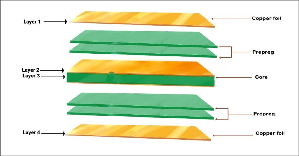
- Prepreg
One pre-impregnated sheet is a prepreg consisting of resin and reinforcements. It’s the adhesive layer that holds the PCB cores together, ensuring the layers bond well. During lamination, the resin in the prepreg flows out and cures again, binding the layers fairly firmly yet durably together.
- Core
The core is the rigid base material of a PCB, generally made of FR4 composite materials containing epoxy resin and fiberglass. Wide usage of FR4 applies due to high mechanical strength, good thermal stability, and electrical insulating characteristics.
In this manner, the substrate core maximizes structural rigidity and stability for the PCB as the backbone in the making of the laminated board.
- Copper Foil
Copper foil refers to thin sheets of copper applied on the outer layers of the PCB. These foils are used for electrical conductivity and allow the carrying out required operations within the PCB.
The copper layers form the electrical pathways as they connect the different components; thus, electricity can flow through them, enabling the PCB to work accordingly.
Now you know the basics of PCB lamination, it’s time to learn the PCB lamination process in detail.
PCB Lamination Process
Here are the steps involved in the PCB lamination process:
Step #1: Preparation
The first step of lamination involves preparation. This is for the core surface and copper foil cleaning and preparation.
Any contamination—dust or oil should be eliminated in readiness for adhesion. Surface preparation ensures that the materials are correctly joined to form a cohesive unit.
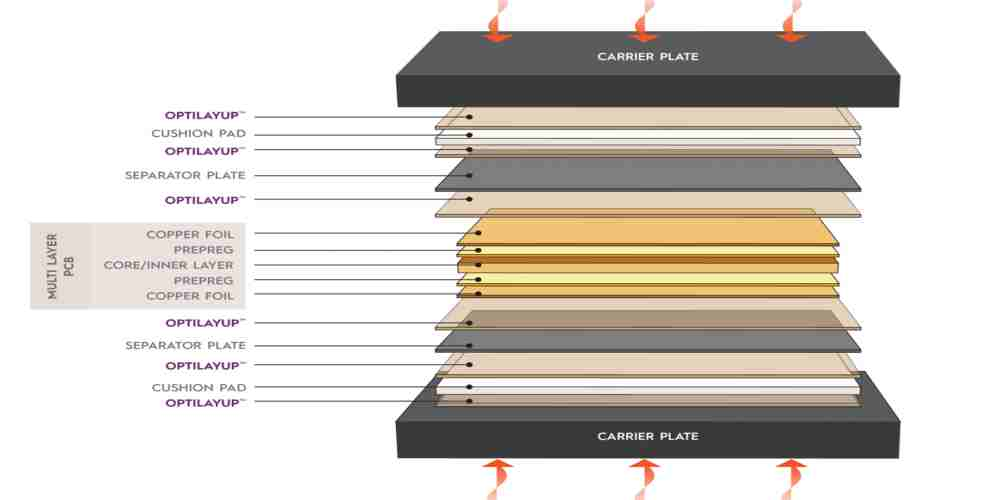
Step #2: Layup
The following process involved is a layup. The step consists of laying the prepregs, cores, and copper foils, one on top of the other in the correct sequence as stipulated by the PCB design.
The layup sequence is quite a critical process, as it affects not only the final structure but also the functionality of this printed circuit board.
Ensuring all layers are correctly aligned and positioned to offer electrical and mechanical properties as required is therefore essential.
Step #3: Lamination
Once the layers are stacked, the lamination process begins. At this step, depending on the method of lamination selected, press lamination, vacuum lamination, or autoclave lamination—heat and pressure (and probably vacuum) are applied.
This stage binds the layers together by flowing and curing the resin in the prepreg into a solid, unified PCB.
Step #4: Curing
After lamination, an assembly undergoes a curing process. The applied pressure and temperature are held for some time to complete the adhesive bonding.
Proper curing guarantees the integrity and durability of the laminated PCB since the resin fully hardens, and layers will be held in place.
Step #5: Inspection
Inspection is the last step in the lamination process of a printed circuit board. The defects that could be misaligned in the laminated board, such as voids or delamination, are checked.
This is a critical quality check procedure for the board to assure conformance with specifications and function. Any anomaly detected in this stage and subsequent rectification will prevent field failures and ensure reliability in the finished product.
Design Considerations for PCB Lamination
Here are some critical design considerations that will help during the process:
Layer Registration
Accurate alignment of the different layers in a PCB refers to layer registration. Proper registration is done to ensure signal integrity and functionality. Misregistration produces signal loss, crosstalk, and general degradation in performance.
Correct positioning of every single layer in a PCB in relevance to one another keeps electrical pathways and circuit design characteristics intact.
Stackup Design
The stack up design refers to the definition of the thickness and material for any layer in the PCB. The design considerations are driven by the finished product’s electrical and mechanical requirements.
Proper planning of stack up will ensure that the printed circuit board can take up the necessary current loads, maintain signal integrity, and live through mechanical strength as required.
Thermal expansion/contraction can be controlled to avoid warpages and other mechanical issues.
Hole Tolerance
The hole tolerance is directly proportional to the diameter of the drilled hole and the accuracy regarding the positioning of the said holes. In a PCB, such drilled holes are known as vias.
They connect all or some layers inside a populated board to facilitate the passage of electrical signals. For correct via formation, proper care must be taken regarding the size of the hole and its positioning.
Otherwise, when hole tolerance is poor, this will misplace the vias in the board, which in turn might result in electrical connectivity problems.
Quality Control in PCB Lamination
Quality control is crucial in the PCB lamination process:
- Electrical Testing: Conduct electrical tests to identify potential shorts or opens in the circuit. This ensures the PCB functions correctly.
- Visual Inspection: Check for defects such as delamination, voids, or warpage. Visual inspection helps catch issues early on.
Microscopic Inspection: Use microscopic inspection to ensure proper layer registration and via formation. This level of detail helps verify the integrity of the lamination.
Troubleshooting PCB Lamination Defects
Even with the best designs and careful execution, defects may still occur in the PCB lamination process.
Listed below are some of the more common defects related to PCB lamination and their possible solutions:
1.Delamination
Delamination refers to the loss of structural integrity and electrical performance when the various layers of a PCB come apart. Reasons may include excessive pressure, temperature, or poor quality of prepreg.
Prevent delaminations by selecting the proper approaches to apply pressure and temperature during lamination, following good-quality prepreg, and taking due care in material handling.
2.Voids
Voids are small pockets of air between layers of a printed circuit board. They result in structural weakness of the board and sometimes lead to electrical failures.
Such defects as insufficient pressure, layup techniques, or unsuitable prepreg may accompany them.
Eliminate the issue of voids through evenly distributed pressurization, vacuum lamination as required, proper material preparation, and alignment.
3.Warpage
Warpage, in simple terms, is uneven bending of the PCB and can cause functional limitations. It is mainly caused by incorrect core material, differences in thermal expansions, and harmful clamping.
Avoid warpage by selecting compatible core materials, designing for perfectly balanced thermal expansion, and applying even clamping pressure during lamination.
Final Words
In conclusion, understanding PCB lamination is crucial for making strong and reliable printed circuit boards. By learning about the lamination process and its importance in creating durable circuits, you can choose the right techniques and materials.