As we all know Internet of Things devices are, basically, connected devices that improve their collective functionality through data sharing. IoT connects and interlinks actual objects using sensors and software with the internet.
Since they form the structure that, together with the connections, gives a device the capability to process data and communicate, printed circuit boards are certainly one of the most critical components of any IoT device. They will house parts such as sensors and communication modules to ensure everything goes well in an IoT system.
In contrast to traditional PCB, designing for IoT is an entirely different activity. The design of the PCB for the IoT application includes a sensor and wireless modules like WiFi with low power consumption, small in size, with high reliability and toughness in different environments.
For the proper functioning of devices in an IoT context, designers consider efficiency, signal strength, and ease of making.
Designing PCBs for Internet of Things devices is unique and presents challenges that must be considered if the best possible performance and reliability are to be obtained.
With the small size and low weight of things or objects in the IoT world, like wearables and sensors in particular, it requires smaller and lighter PCBs. Miniaturization is then compulsory to integrate complex functionality into a package constrained by limitations.
In devices using IoT, the draining of the batteries has to be prevented, and hence, the PCBs should be designed with the least possible requirement for power consumption. More efficient techniques in power management are therefore necessary to bring out maximum life during operation.
Integrating wireless communication modules like Bluetooth, Wi-Fi, and cellular into IoT PCBs will require proper planning concerning seamless connectivity and interoperability.
Efficient integration of antenna ensures perfect and reliable wireless communication within the constraints set forth by the size and form factor of the IoT devices.
IoT devices are generally used in diversified and, at times very harsh environments. Accordingly, the PCBs should be designed to work amidst various conditions involving extraordinarily high or low temperatures, humidity, and mechanical vibrations.
Since IoT devices are used to transmit and process sensitive data, appropriate protection against impending threats is critical. Robust security measures should be incorporated into this PCB design.
These challenges can be overcome by careful design and engineering to ensure that IoT PCBs are not designed merely to meet application requirements but function well for real-world applications as well—thereby enhancing the functioning and lifespan of a prospective IoT device.
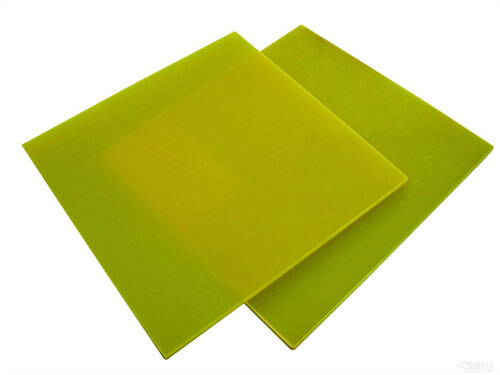
Choosing PCB material should be calibrated to ensure reliability and performance for IoT devices.
Here’s what needs to be considered:
The selection of a suitable PCB material will take into account all these factors to optimize the performance, reliability, and life span of IoT devices for designers.
Heat generation management is very critical in densely packed IoT PCBs for achieving reliability and long life.
Here are some effective strategies:
Choosing appropriate materials for the PCB with high thermal conductivity for efficient heat dissipation is done.
It enhances heat management in a way by providing materials like metal core PCBs or those having copper inlays that quickly transfer the heat away from components generating much heat.
Attach heat sinks to hot components and thermal vias on the PCB, which allows heat dissipation. Heat sinks increase surface area for dissipating heat, while thermal vias improve heat flow between layers of the printed circuit board.
Careful placement of components on a PCB can ensure good air velocity and heat dissipation. Keeping all the heat generators together on one side of the board, near the edges, or directly in the path of airflow will help minimize heat buildup and enhance the efficiency of cooling.
Efficient power management is crucial for making IoT devices last longer on batteries and work reliably. Here’s why it’s important and how to do it right:
Due to the ordinarily battery-powered nature of IoT devices, their power efficiency offers several-fold advantages from such improvements regarding the extension of battery life with reduced recharging or replacement cycles.
Efficient power management will also keep the devices cool, which impacts the performance and durability of the devices.
Following these steps will efficiently manage the power in your IoT devices and make them more reliable, which will eventually save energy and reduce costs.
There are some critical parameters in a PCB for IoT devices other than power management.
Here’s what else to consider:
Select low-power components that can be fitted into compact spaces. This ensures their efficiency without a lot of room intake.
Both keep signals solid and clear, especially the tiny devices bound to be interfered with. Good PCB layout and shielding techniques help maintain signal quality.
Test your PCBs properly to work well, use power wisely, and be reliable. Run simulations against real-life situations to conduct the tests to detect any error at the very beginning.
Design PCBs that are easy and cost-effective to manufacture. Consider how parts go together and how they can be assembled quickly during the manufacturing process.
Given such considerations in design, you can obtain IoT devices that turn out to be reliable and efficient in performance towards meeting the needs of different applications.
So that’s all you need to know about IoT PCB manufacturing and assembly. Whether you’re new to IoT or have experience, following this guide will help you build efficient and durable IoT devices.
By focusing on these aspects, you’ll be able to meet the needs of various applications effectively. With careful planning and implementation, you’ll be on your way to developing successful IoT projects that perform well and last long.
We are committed to making our products zero-defect and can return or exchange them for you without any reason.
Fill in your requirement information and upload Gerber and BOM files, we will give you a quote within 24 hours.
Fill in your requirement information and upload Gerber and BOM files, we will give you a quote within 24 hours.