How to solder multilayer PCB might seem tricky, especially if you are used to simpler boards. With multiple layers and complex designs, it can be challenging. However, do not worry; this guide will break things down for you in simple steps clearly explained.
Having problems with component placement or maybe soldering? We understand. By the time you’re reading this, you’ll be confident and ready to take on multilayer PCBs with ease.
So, let’s get started.
Understanding Multilayer PCBs
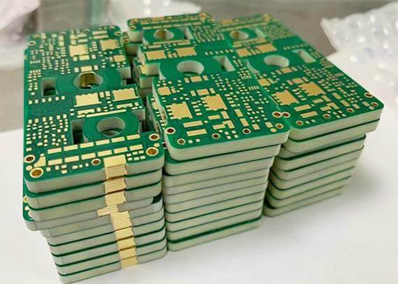
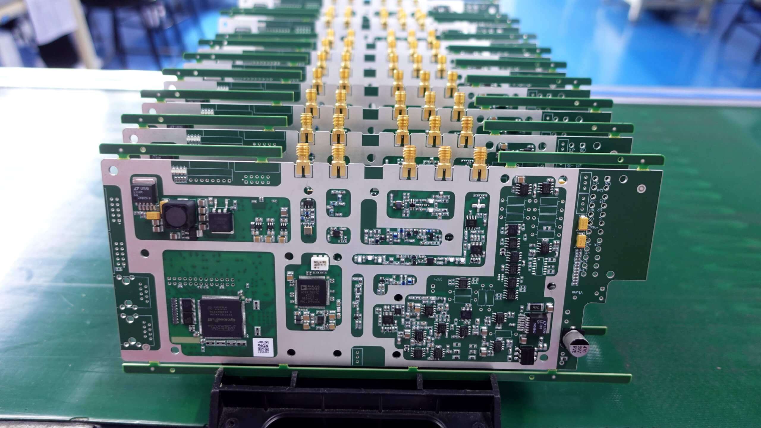
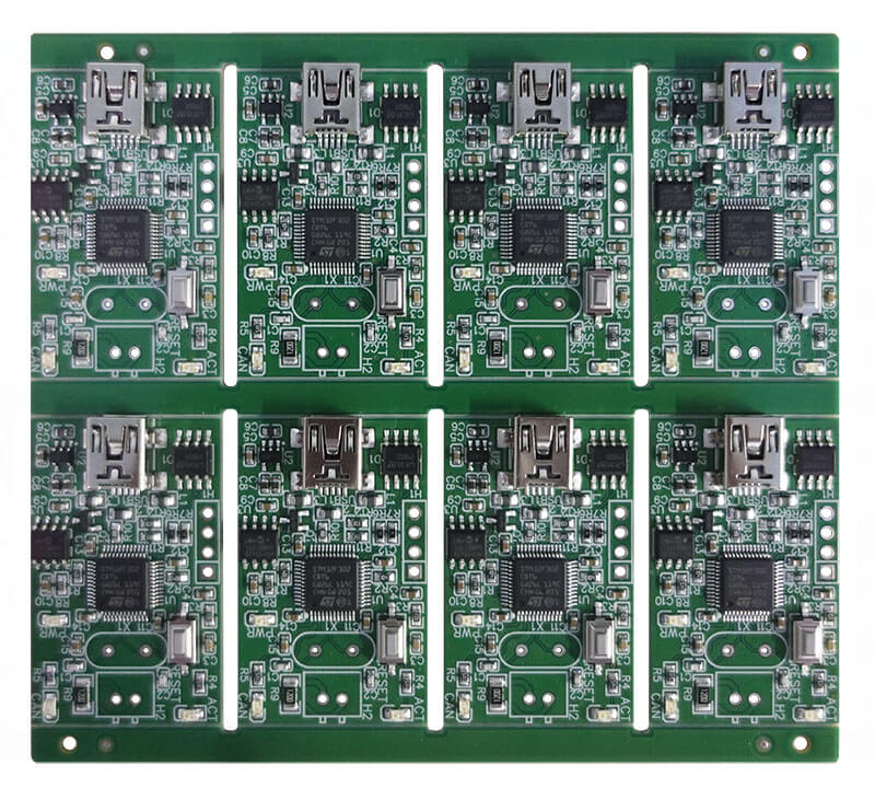
Multilayer PCBs are used in many modern electronic devices—from smartphones to hospital devices. Due to the multilayer design, in contrast to a single-sided or double-sided PCB, more complex circuits can be laid out within a given small area.
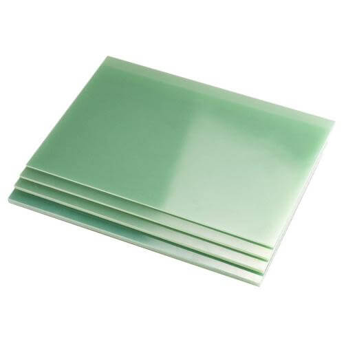
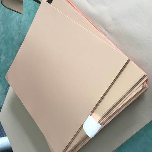
A multilayer PCB typically consists of copper and insulation material, such as fiberglass, in different layers. Such layers are pasted together, then holes are drilled through to electrically connect the layers.
Now, the main advantage of multilayer PCBs is that they are capable of housing more complex circuits within small sizes. On the other side, the same complexity of design makes soldering a bit complicated because you have to reach and solder each layer carefully.
Challenges of Soldering Multilayer PCBs
Soldering multilayer PCBs could be more complex compared to the easier boards, which have a simple design. Here are the common difficulties that you may encounter:
- Accessing Layers:When multiple layers are stacked, the inner layers may be inaccessible for making and soldering connections. Special tools and techniques often have to be used to ensure that every layer gets properly soldered.
- Heat Management:Due to the increased prices of multilayer PCBs, there will often be a need to deal with careful heat management. Too much heat can damage the sensitive elements or cause delamination of layers; on the other hand, too little heat can result in weak or unreliable solder joints.
- Alignment Issues:Ensuring that all layers are properly aligned and that holes for through-hole components are correctly placed can be challenging. Poor alignment causes a load of bad connections and loads of soldering issues.
- Soldering Defects:Since multilayer PCBs possess more complexities, they are much more prone to defects like solder bridges, cold joints, and component lifting. Extra care and attention are required for identifying and fixing such issues.
Now let’s learn how to solder multilayer PCB in detail.
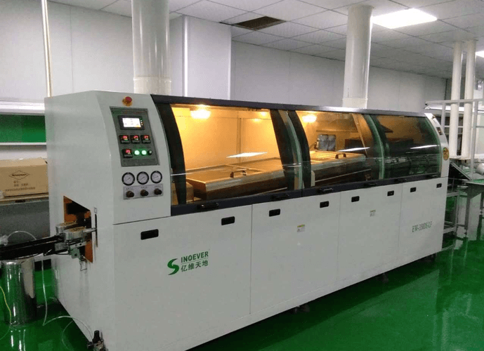
Soldering Equipment and Materials
To solder multilayer PCBs effectively, you need the right tools and materials.
Here’s a list of what you’ll need:
- Soldering Iron or Station:A good soldering iron with a fine tip; with adjustable temperature.
- Solder:Use lead-free solder or leaded solder, depending on your needs. Ensure it has a flux core.
- Flux:Apply flux to help solder flow smoothly. No-clean flux is best to avoid residue.
- Desoldering Tools:Have some solder wick or a desoldering pump to fix your mistakes.
- Tweezers and Pliers: Use tweezers for small components and pliers for positioning and bending leads.
- Heat Gun or Preheater: These are some of the tools that are used to warm the board.
- Cleaning Supplies:Isopropyl alcohol and brushes are used to clean the board after soldering.
- Inspection Tools: These either incorporate magnifying devices or a microscope for the close-quarter inspection of the solder joints.
Soldering Techniques
Here are some key techniques for soldering multilayer PCBs effectively:
- Component placement: Place the components carefully and align them with the pads on the board. Align precisely with tweezers.
- Preheat:Gently heat the board using the heat gun or preheater to ensure less thermal stress, which makes the job easier in terms of soldering.
- Solder Application: Add solder to the joint while heating both the pad and the component lead. Remove the iron after the solder flows smoothly and evenly.
- Cooling: Allow the solder to cool off without disturbing it. This will ensure strong and reliable joints.
- Inspection:Each solder joint is carefully inspected for uniform flow and no defect is present with the aid of a magnifying tool or microscope.
- Cleaning: After having soldered, remove any flux residue or debris from the board by cleaning it with a spirit-soaked rag or isopropyl alcohol and a brush.
Common Soldering Defects and Solutions
Here are some typical soldering defects you might encounter with multilayer PCBs, along with solutions:
1)Solder bridges:
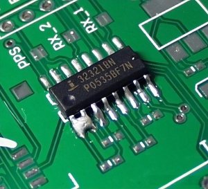
When excess solder connects two or more pads unintentionally.
- Solution: Clean off excess solder with the soldering iron and solder wick. Check to ensure that no bridges exist.
2)Cold Solder Joints:
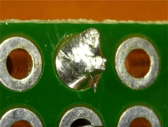
These will appear as either dull or weak connections; these usually happen due to a lack of enough heat.
- Solution: Re-flow the joint and add a little solder if necessary. This time make sure that the pad and lead are adequately heated.
3)Component Lifting:
Components can possibly lift off the board if the solder joint is too weak.
- Solution:Reheat the solder and press the component back into place until the solder solidifies. Check the joint for strength.
4)Tombstoning:
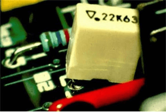
When one end of a component lifts off the board, while the other remains soldered to it.
- Solution: Avail uniform heating, and also make sure there is enough solder at both ends of the component. Reheat and readjust as needed.
5)Opens and Shorts:
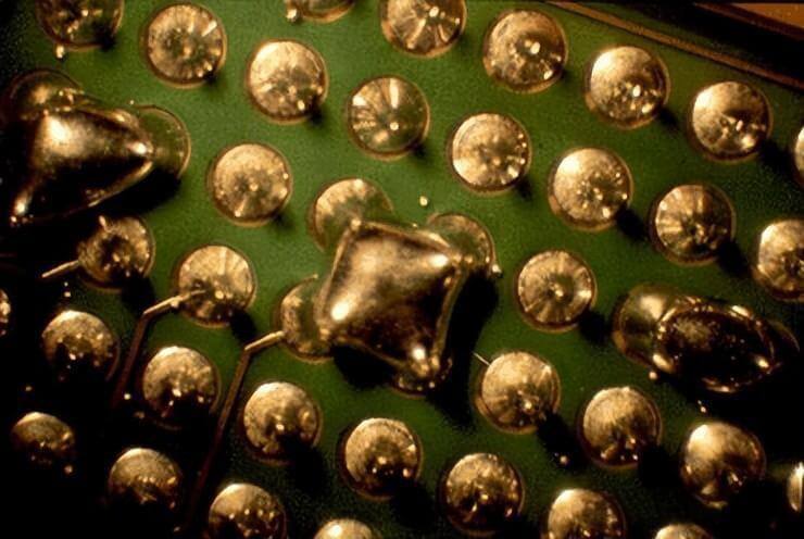
An open is a broken wire; a short is an unintended wire.
- Solution:Use a multimeter to check for continuity. Rework the affected joints to fix broken connections or remove unintended solder.
Conclusion
Soldering multilayer PCBs might seem tough, but it gets easier with the right tools and techniques. We hope this guide has helped you understand everything about the process along with the tools you need.

