


Are you also tired of this continuous concern, noise in PCB design? Well, you are not the only one. As electronics enthusiasts and engineers, we know how much trouble noise can cause to our electronics circuits.
Be it distortion, errors, or just unpredictability: noise in PCB design can turn out to be an eyesore. But have no fear as help is here.
The following step-by-step guide will navigate through proven strategies for noise reduction in PCB design. Besides, we will also discuss the sources of noise in PCB designs so that you can be able to understand how to get rid of it.
Let’s dig into it.
Understanding Noise in PCB Design
Before going straight to ways of how to reduce noise in PCB design, the first thing to know is what noise is.
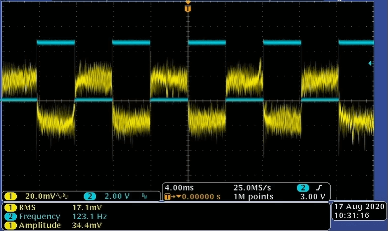
Noise in PCB design is considered to be any undesirable electrical signals that tend to interfere with the proper running of the circuit. This may come from different sources, which might include electromagnetic interference, crosstalk from neighboring traces, or ever-changing power supply voltages.
Noise does have a very large influence on signal integrity; in digital communications, it can distort the signal waveform in error and degrade the quality of analog signals.
For example, in high-speed digital circuits, the smallest timing error induced by noise can be the cause of data being recorded erroneously.
By now you must be getting a thought that why such noise elimination is required in PCB designing. Let’s see this in detail.
The Importance of Noise Reduction in PCB Design
The importance of noise reduction in PCB design cannot be overstated. A circuit’s reliability hinges on its ability to function without interference from noise.
This involves proper grounding, decoupling capacitors, and trace routing, as some of the noise reduction approaches.
These are practices that ensure the PCB delivers its desired function, even with potential noises from sources.
In fact, with the advance of miniaturization and integration of electronic devices, it is increasingly difficult to control noise, and that is the very reason why in today’s PCB design, the principles of noise reduction have assumed more relevance.
But what are the sources of noise in PCB design? Let’s discuss this in detail.
Sources of Noise in PCB Designs
As said earlier, noise may arrive from any source, each of which has the power to degrade signal integrity and therefore circuit performance in most ways.
Below is a list of some very common sources that you should be aware of in order to reduce it.
- Power Supply Noise
What should also be rated as a big noise factor is the power supply, which may be thought of as the heart of any electronic system. Voltage levels or power distribution irregularities can inadvertently couple to signal lines and therefore introduce undesired noise to sensitive components.
- Grounding Noise
Proper grounding will ensure electrical safety and function, while poor grounding practices will have pure assurance of noise on our circuits. Such ground currents will result if a difference in ground potential occurs at different locations in the circuit, leading to unwanted currents and consequently noise.
- Crosstalk
In electronic terms, crosstalk is like an overheard conversation. If nearby traces on a PCB start acting like unintentional antennas, they might pick up electromagnetic interference from each other.
This EMI can induce unwanted signals that corrupt the intended communication between components. It would be more apt to say if these traces are whispering secrets to each other—in other words, the message gets corrupted.
- Electromagnetic Interference (EMI)
Even external sources of electromagnetic interference, like electronic devices nearby or power lines and radiofrequency transmissions, could affect the performance of the PCB.
These are all different elements of noise disturbances that come from the environment and make the task of reducing noise more complicated.
This enables the identification of sources of the noise and what might go wrong to be a potential weakness in design for our PCBs.
By knowing these sources, we will be able to apply concrete strategies to target the reduction of noise and ensure that our circuits operate appropriately.
How to Reduce Noise in PCB Design
Reducing noise in PCB design requires a multi-faceted approach that addresses various sources of interference and implements targeted strategies to mitigate their impact.
Here are some useful ways to get cleaner and more reliable circuits:
1.Grounding and Shielding
Proper grounding practices are foundational to noise reduction in PCBs. By strategically establishing numerous grounding points on the board, engineers create low-impedance paths for returning currents, thereby reducing the risk of ground-induced noise.
It is opined that one of the most common sources of noise is ground loops, resulting from multiple ground paths and which, in turn, create unintended current flows.
So, here, there exists the potential of signal distortion or interference. This is one area where the engineers pay enormous attention to all details in the design of the grounding scheme so that perfect connectivity is maintained and ground loop formation is minimized.
Besides, shielding techniques are the most important for neutralizing the effects of interference, whether self-generated or picked up.
By simply placing barriers around sensitive components or signal traces that have been created using conductive materials such as copper foil or metal enclosures, engineers literally encase elements within a barrier that blocks electromagnetic interference (EMI).
2.Decoupling Capacitors
Decoupling capacitors are used to store the charge required in ICs for the current switching circuit during high-speed transitions made by the voltage.
These capacitors are placed adjacent, strategically close to the power pins of ICs and other sensitive components. The capacitors stabilize the distributed voltage on the power pins, by reducing fluctuations of voltages, and invariably reduce noise.
This is normally done by the use of ceramic and tantalum capacitors because a large value of capacitance and fast response time are their characteristics.
The selection of the right kind of decoupling capacitors should consider capacitance, voltage rating, and frequency response such that effective noise filtering is achieved under all working conditions.
3.Power Plane Design
Power plane design should be strong to achieve uniform power distribution on the PCB, which helps reduce voltage drop and noise. Power planes are therefore traced as a low impedance path that conducts power uniformly through all components so as to maintain one common voltage plane and hence prevent local voltage fluctuation, hence preventing the noise.
Good separation between power and ground planes is highly important to reduce signal interference and crosstalk.
Adequate spacing is maintained between the power and ground planes to lower electromagnetic coupling, thereby minimizing the noise-induced distortion of signals—an aspect that is very critical for high-speed designs in so far as signal integrity is concerned.
4.Signal Integrity Practices
Controlled Impedance Routing is one of the basic techniques in high-speed PCB design to maintain signal integrity. Impedance matching is done to establish conditions in which the impedances between the source and the channel, the channel itself, and the channel and the receiver are all equal.
All these factors contribute to reliable signal transmission and reception, even in environments with a lot of electromagnetic interference.
Other careful trace routing techniques include optimization of trace spacing by minimizing trace length, and the avoidance of sharp bends, thereby further enhancing coherent integrity by making it less likely that noise will couple between adjacent traces.
Another vital characteristic is that it reduces common-mode noise, therefore making it provide better immunity from noise for high-speed communication interfaces.
If these techniques are used wisely in the PCB design, it will be able to eliminate noise, improve signal integrity, and assure reliable operation of electronic circuits for many applications.
The Advanced Noise Reduction Techniques
If you are an experienced PCB designer looking for techniques to reduce noice, here are some advanced techniques that can help you:
1.Filtering
Filtering is, therefore, the best way when it comes to attenuation of specific noise frequencies, which cannot be attenuated to an allowable level by any other conventional means.
The presence of low-pass, high-pass, or band-pass filters in the PCB design can make noise suppression intelligent without signal integrity being affected.
Advanced filter designs using active filters and DSP algorithms provide better adaptability and precision to target noise frequencies, solving complicated noise problems in high-performance circuits.
2.Signal Termination
Signal termination techniques are used to minimize signal reflections while maintaining the integrity and quality of a signal in high-speed designs.
Some of the examples of advanced termination schemes are series termination and parallel termination. It ends the impedance to the load impedance in the transmission line and thus averts signal bounce while also minimizing noise-induced signal distortion.
Moreover, stub termination or AC coupling gives even more fine-tuning in controlling signal reflections for optimized signal quality; apart from that, the technique is certainly required by more demanding applications where the noise margins are close.
3.Simulation Tools
Simulation tools are essential in simulating and analyzing noise behavior in PCB designs before fabrication. The inclusion of leading-edge simulation software, integrated into the PCB design tool, allows an engineer to model and simulate proactive noise scenarios for a complete analysis and optimization of noise reduction strategies.
By simulating signal integrity, power distribution, and electromagnetic compatibility, engineers can identify potential noise hotspots, evaluate the effectiveness of techniques for noise reduction, and iteratively refine their design for optimal performance.
With such strong improvements in noise reduction techniques, a design engineer with good experience in PCB can push forward into the wilderness of performance and reliability in design, waging war on even the most difficult noise issues boldly and specifically.
Conclusion
So that’s how you can reduce noise in PCB designs. All you have to do is follow the strategies and techniques given above and you will end up with an effective PCB design according to your project requirements.
Implementation of these methods by an engineer would also assure that the circuit would function smoothly and reliably.