Do your stencils not align right when you use them in your PCB assembly? That sure can be a mind-blowing process, bringing up all forms of soldering issues that mess up the whole assembly.
But don’t worry. This article has got your back. We are here to walk you through the whole puzzle of stencil alignment, step by step. After you learn how to get it right and understand why it’s important, you will have nothing between you and smooth, flawless solders every time.
So let’s get started.
The Role of Stencils in SMT PCB Assembly
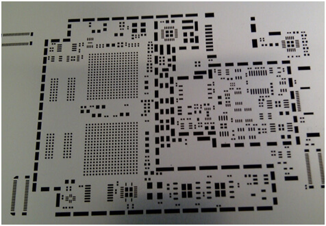
Before getting straight to the PCB stencil alignment design, one must first understand what a stencil does in SMT PCB assembly.
Stencils are very important in Surface Mount Technology PCB Assemblies as they help in depositing the solder paste accurately on PCBs.
Here’s how they contribute:
- Putting Solder Paste: A stencil is responsible for spreading solder paste, which will eventually form joints for your components. As a result, stencils will contain tiny holes that are to be aligned over the pads on your PCB.
- Amount Control: Stencil controls the right amount of solder paste applied to each pad, thus ensuring even solder joints and eliminating problems resulting from too much or too little solder.
- Getting It Lined Up: Stencils aid in aligning the soldering paste applied to a printed circuit board over the pads so everything can be soldered in the right place.
- Cost Savings and Time: Though stencils will cost money at the start, in the end they will save cash through preventing errors. They also make things go faster by the ease of applying solder paste.
That is to say, stencils act like an extra pair of hands to ensure that solder paste goes only where it needs to go so that the entire assembly process is smooth and reliable.
Key Design Elements in Stencils for Alignment Accuracy
Now, after learning the importance of an accurate alignment of the stencil, let’s go into two main design elements that affect this property within stencils.
- Fiducial Marks: These marks are like guiding stars, and are pivotal for automated alignment. Placed on both stencil and PCB, they serve as reference points, ensuring precise positioning during printing.
- Registration Holes (Optional):They are the second way of providing fine clearance because they do not need precise drilling in both the stencil and PCB like in the use of fiducial marks to provide accuracy in alignment.
- Stencil Dimensions: It is very critical that all the dimensions perfectly line up with the PCB dimension. Discrepant dimensions may yield paste deposition in wanted areas, and consequently others of soldering defects. This will ensure a good fit of the stencil and prevent this kind of occurrence.
Alignment of the stencils is one of the most important design elements for building a strong base during PCB assembly.
Techniques for Stencil Alignment
Now that we have learned a few of the major design elements and/or decisions in stencils, let’s have a look at some of the actual methods for making sure there is proper alignment when assembling a PCB:
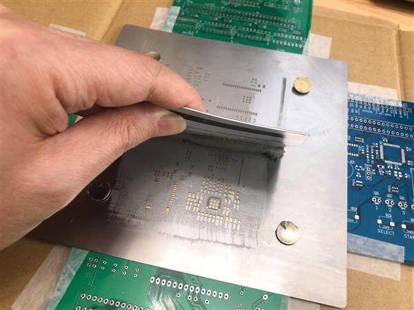
- Automated Stencil Printers: These are high-end machines that employ camera vision systems in easily centering the stencil in relation to the fiducial marks. This establishment achieves rapid and efficient alignment; hence, the most appropriate technology for high-volume production.
- Manual Alignment (for Low Volume): In a low-volume situation, manual alignment techniques are necessary. This could utilize such features as locating pins, or this could be an entirely visual operation to get the stencil registered to the PCB. It may be a bit less automated and a lot more delicate, but manual alignment may be just as effective.
These techniques will enable manufacturers to ensure that stencils are aligned with accuracy, hence laying the base for a good quality PCB assembly.
DFM Guidelines: How PCB Design Choices Can Impact Stencil Alignment
DFM is therefore critical for manufacturability in optimizing the alignment of stencils for PCB assembly.
Let’s consider some test cases where PCB design decisions can affect the outcome of stencil alignment process greatly:
1.Fiducial Mark Placement
This requires careful strategization in order to achieve the correct alignment of stencils. It also involves a few other guidelines to ensure that the surfacing of the marks is toward the automated systems setup for their respective visible recognitions.
This ensures that the process of alignment is fast and reliable.
2.Component Placement
The density and size of the components in the PCB will determine how the stencil is to be handled and aligned during the printing. In the case of overly packed layouts or oversized components, the stencil might block out the surrounding space, complicating the alignment.
In precision designs, components can be placed in a manner that eases alignment and printing.
Common Challenges Encountered During PCB Stencil Alignment
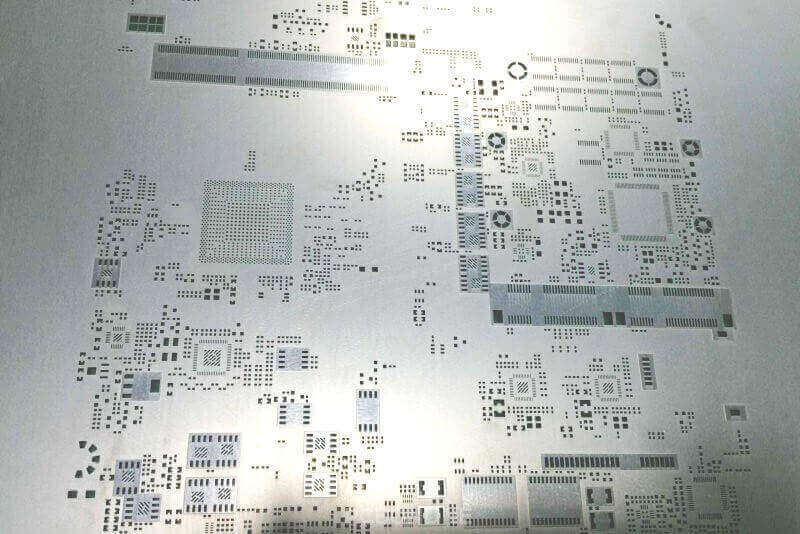
Despite your best efforts, there can sometimes be issues within a PCB alignment of the stencil.
The following are some of the most common issues, as well as solutions to them:
- Misaligned Fiducial Marks
Sometimes the fiducial marks are not placed correctly at the time of placement due to slight manufacturing inaccuracies or faults in design. This leads to the scenario where the paste stencil may be misaligned and, as a result, has defects during soldering.
Make sure to double check on the exact place where fiducial marks are supposed to be placed before designing the PCB. Make sure they are visible enough when manufactured.
- Stencil Warping
The warping of the stencil, mostly because of bad handling or poor material, results in a deviation from the accuracy of alignment. The warping of the stencils will not lay flat on the surface of the PCB, thus yielding uneven deposition of the solder paste.
This can be overcome by ensuring that the materials used for the stencil are high in quality, and, during the use, they are stored and handled carefully.
Conclusion
So, getting your PCB stencil alignment right is super important for making sure your assembly goes smoothly and your soldering turns out great.
By understanding the role of stencils, knowing what design elements to look for, using the right techniques, and dealing with common issues, you can make sure everything lines up perfectly.

