


Ever wonder how devices that are so complex can still fit together without taking up a larger space? Multilayer PCBs are the secret. Simple PCBs may have one or two layers. However, multilayer PCBs contain three or more conductive material Layers. This enables them to deal with more advanced and powerful designs.
So, what makes multilayer PCBs so important? They help you pack more functionality into limited space. They can handle more complex circuits, from noise reduction to better signal quality.
Multilayer PCB design involves planning, creating, and placing electric connections across several layers. This is very important for building high-performance devices. This post will walk you through the process of designing multilayer PCBs. Let’s get started!
Essential Steps In Multilayer PCB Design
Designing a multilayer PCB can be complex, but fear not! You can create a sturdy and strong board with careful planning. Let’s discuss the essential steps to make this process smooth and manageable. Here’s how you can get started:
#1. Defining Project Requirements:
First, you need to define what your project needs. Here’s what to consider:
- Functionality of the Circuit: What do you want your circuit to do? If you know how it is used, it will influence your design. Now, you can just think about the circuit functions that need to go into it. For power management, signal processing, and control systems. This is to understand clearly what the components and layouts needed.
- Component Selection and Placement: Choose components that fit within your board dimensions and performance requirements. Proper placement contributes to design optimization. By keeping high-speed components together, you can minimize timing delay. Separate analog and digital for noise reduction.
- Performance Specifications:The design must meet Signal integrity and power requirements. It requires high-speed signals and good power distribution. Signal integrity means keeping electrical signals clear. Stable power distribution to all the components avoids noise and ensures reliability.
#2. Choosing the Right Number of Layers
The number of layers must be chosen carefully. There must be balance in manufacturability, cost, and complexity. This is how you go about it:
- Balancing Complexity and Cost:Complete the design with fewer layers. More layers increase complexity and cost. Strive for the minimum number that is still effective.
- Signal Routing and High-Speed Signals:Extra layers are needed for high-speed signal routing and integrity. Carefully plan your layers to manage signals. Separate power and ground layers to minimize noise and enhance signal integrity. Route adjacent signal layers in opposite directions to reduce crosstalk.
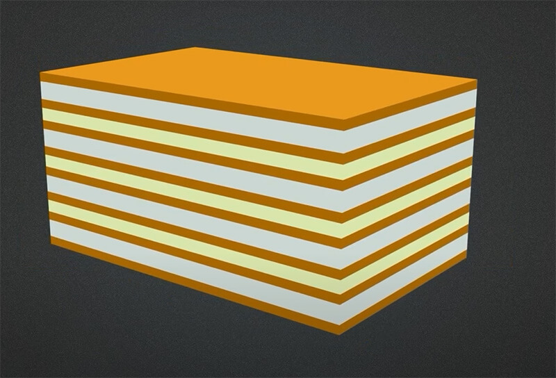
#3. Layer Stackup Planning
Best performance and reliability depend on careful consideration of your layer stack-up. This is how to do it efficiently:
- Arranging Signal Layers and Planes: Systematically arrange your signal layers, power, and ground planes. Place high-speed signals on internal layers between power or ground planes. This setup reduces noise and improves signal integrity. Keep analog and digital signals separated to avoid interference.
- Optimizing for Signal Integrity and Noise Control: Power and ground planes shield noise signals. They create point-to-point power distribution rails. Also, ground reference points for signal return paths. This reduces noise from electromagnetic interference and increases performance. Power and ground planes must be close together to act as capacitors, enhancing signal quality.
#4. Schematic Capture and Symbol Selection
A successful design requires the creation of a comprehensive schematic. Here is how to do it;
- Using PCB Design Software: Use reliable PCB software that shows your circuit accurately. The software maps every part and connection. It ensures that all circuit parts are properly connected. Also provide a clear structure for the layout.
Selecting Symbols: Pick the right symbols for each element to clarify things and prevent errors. Make sure that pad shapes are accurate for the inner layers. Some versions use different shapes in the outer and inner layers. Checking these details is what prevents errors.
#5. PCB Layout and Routing
Layout and routing are very important for signal integrity and working. Here’s how to do it right:
- Placing Components:Place components on appropriate layers according to function and signal flow. Group components to keep related parts together. This reduces trace lengths and increases performance. Keep your high-powered, noisy components away from sensitive ones to reduce interference.
- Routing Signal Traces: Make a good route trace to keep free signals and avoid crosstalk. Make it short and clear to avoid signal loss. Use wider traces for power and ground to reduce resistance and voltage drops. There should be proper distance between layers of traces to prevent interference.
#6. Design for Manufacturability (DFM)
Designing a product that can be easily manufactured is very important. Making sure that it must follow the industry standards and manufacturer guidelines. Here’s how to do it:
- Adhering to Manufacturer Capabilities:Stay within your manufacturer’s design capabilities. This includes clearances via sizes and minimum trace widths. Every manufacturer has their limit. So, you will need to verify the specifications of each one before finalizing your design. This avoids problems during production and keeps costs down.
- Following Industry Standards: Design according to standards ensures that your PCB will be reliable. It is free from production issues. Conform to spacing/trace width rules and via positioning. Remember the rules for spacing, trace widths, and via placements.
#7. Design Rule Check (DRC) and Electrical Rule Check (ERC)
DRC and ERC are the process to find issues in your design before fabrication. Here is the proper way to use them effectively;
- Using Software Tools:Run DRC and ERC in your PCB design software. These are the automated tools to check your layout. DRC checks for physical issues such as spacing, trace widths, and clearances. ERC is for electrical verification, such as short circuits, isolation open pins, and signal paths. These checks help us catch errors in your board that could lead to a failure.
- Correcting Errors: Resolve any errors or issues caught by these checks. The software will identify the areas where you are going wrong and help you rectify them. Correcting these areas ensures your design is ready to be manufactured. It prevents problems and saves money and time.
#8. Gerber File Generation and Fabrication
Once your design is complete, you must generate Gerber files for fabrication. Here’s how to do it:
- Generating Gerber Files:Create Gerber files for all the layers of your PCB. These contain all the information the maker needs to create your board. Each layer, such as copper layers, solder mask, and silkscreen, has its own file. Double-check that everything is accurate. Any mistake can cause production issues.
- Choosing a Fabrication Service: Select a high-quality PCB fabrication service. Check who has the best reviews and quick delivery times. Ensure they meet all your requirements related to your layout’s layers, traces, etc. Choosing a reputable manufacturer will produce your boards to the highest quality.
Additional Considerations
Designing a multilayer PCB involves more than just basic steps. Here are some additional points to keep in mind:
1.Use Appropriate PCB Design Software:
Select a PCB design tool that allows multilayer designs. Opt for layer stackup planning, routing utility, and DRC/ERC. These features allow you to easily organize layers, route signals, and verify structural integrity.
Good software makes it faster and more manageable. It can catch errors early and save time and money.
2.Signal Integrity and Noise Contol:
Maintaining signal integrity and reducing noise is crucial in designing a PCB. To avoid signal reflection and loss, impedance should be matched to your traces. Solid ground planes with short, direct paths to the regulator are good for noise immunity and signal quality. Place vias carefully to avoid disrupting signal paths and to connect different layers to prevent interference.
3.Advanced Techniques for Expert PCB Design:
These techniques must be put into consideration for more complex designs. Signal loss and crosstalk can be minimized while routing high-speed signals. Maintain signal quality through the use of differential pairs and matched length traces.
They are also important in thermal management. Prevent overheating damage by managing heat properly. Utilize thermal vias, heat sinks, and correct layer stackup for heat dissipation.
Final Thoughts:
Multilayer PCB design is not easy, but it can get extraordinary results. Remember, these are the basic steps to get a high-performing board from you. The best practice to design this way is more integrated and transparent.
You should use the tools, collaborate with your fabrication shop, and plan out your designs. The more you practice while paying attention to details, the quicker you can make a multilayer PCB design. Good designs open up new horizons for your electronic projects.