


Do you have an urge to learn how to design a PCB schematic, but you don’t know where to start? You are not alone, because most beginners find the task of converting their electronic ideas into organized schematics very daunting. This step-by-step guide will lead you through the maze of designing a PCB.
We will simplify the PCB schematics by breaking the process down into simple, easy to follow steps. So you can design with confidence.
So let’s get started.
Understanding PCB Schematics
Before we can get into how to design a PCB schematic, we must first understand what a PCB schematic is.
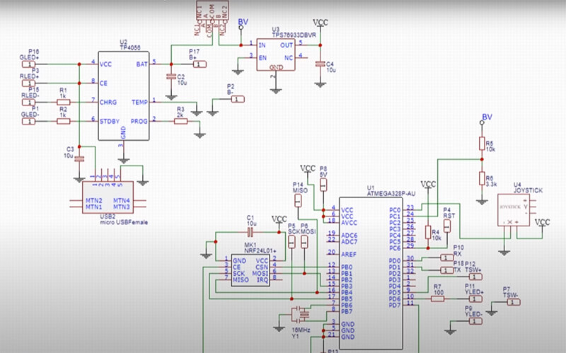
PCB schematics are a fundamental aspect of electronic design; they are the blueprint for the actual construction of the PCB. They are hyper-detailed diagrams used to represent the electrical connections and placement of elements on the PCB. In short, they are the topology of the PCB that will be very important to its proper functioning.
Besides, it acts as a means of communication between engineers, designers, and manufacturers for everyone involved to have an understanding of the intended function and layout of the circuit.
Schematics are one of the major parts in the PCB design process; they run from the conceptualization of an idea to the final manufacturing process. They are the basis on which the whole PCB layout is designed.
Besides that, there some more benefits of PCB schematics that you must know:
- Visualization:Schematics make it possible to visualize the layout of the circuit; very complex designs can be understood and analyzed.
- Error Detection:The schematic is used to detect and eliminate errors and inconsistencies in the designed circuit that can be extremely time- and cost-consuming, and that is done at a very early stage of development, which makes it certain that efficiency is being maintained.
- Documentation:Engineers can return to the schematics for modification purpose and then redesign it as per the requirement.
- Collaboration:Schematics make teamwork possible since they set the standard format of communicating information on design, hence there is easiness in the communication from one design phase to the other.
Now you know the basics of PCB schematics, it’s time to learn how to design it. But for that, it’s important to understand the fundamental components of PCB schematics.
The Fundamental Components of PCB Schematics
Here are the fundamental components of PCB schematics that you must know:
1.Symbols:
They represent electronic parts like resistors, capacitors, transistors, integrated circuits, etc. For every electronic part, there is an assigned symbol depicting its functionality and the way it behaves with electricity.
For instance, a resistor would be in the form of a zigzag line, and a capacitor would look like two parallel lines. This would be of great help to engineers in easily identifying parts and in the way they are placed in the circuit.
2.Nets:
A net is a short form for the word connections or interconnections. It is an electrically conductive path linking different circuit elements within the circuit. Normally, a net indicates a connection between two or more terminals of different symbols representing circuit elements.
A common way of representing nets in schematics is through the use of wires, but there is no limitation in the way nets can be represented.
Each of these nets can carry specific signals in the circuit, like supply voltage, ground, input/output, and clock. Certainly, nets have flows as signals that go through them and electrical connectivity.
3.Labels:
Labels are given to all schematic elements. These are clearly and consistently applied identifications to such schematic elements. Elements that are labeled include components, nets, test points, connectors, and any other appropriate element.
Proper labeling helps understand the function and purpose of each element, making it easier to troubleshoot, maintain, and promote teamwork. It requires clear and consistent labeling to realize accurate and clear schematic design.
Understanding such fundamental building blocks is elemental in becoming capable of designing or understanding PCB schematics in a precise and efficient way.
The Schematic Capture Process
Designing a PCB schematic is an awful lot of work, from tool selections to the effective organization of parts and designing signal flows.
Let’s break it down:
Step #1. Schematic Capture Tools
First, one needs to select the right schematic capture tool. In the market, there are many schematic capture tools, ranging from free to professional packages.
Some commonly used methods are:
- Eagle: A widely-used PCB design software with both free and paid versions.
- KiCad: Alarge, community-supported open-source PCB design tool with a library of components sufficiently large to support it.
- Altium Designer: High-end PCB design software with added features for complex designs.
- OrCAD Capture: Another professional tool that provides the schematic capture capability in total would be OrCAD Capture.
All these tools compete with each other, so you have to choose one according to your budget, your level of expertise, and the requirements of your project.
Step #2. Component Placement
After you have defined the tool, you have to go on to define your components. When you place the symbols of the components into the schematic workspace, you have to consider signal flow, routability, and logical organization.
Group related components together and orient them so that signal crossovers are minimized and routing is easier to perform.
It is also important that enough space is allowed around components for the insertion of notes, labels, and trace routing.
Step #3. Net Connections
Next is the creation of net connections. This is done through using the various tools provided within the schematic capture software. In this step, one usually draws wires or connects lines between pins of different components to represent the electrical connections.
Be very careful about the direction of the signal flow and be entirely sure that everything is correctly connected to its proper destination.
Almost every software tool has options to automatically create net connections and check for the errors of the connections.
Step #4. Power and Ground Symbols
Place the power and ground symbols properly and make a correct connection in relation to each other, as this is crucial to the proper operation of the circuit and signal integrity. Insert power and ground symbols in the circuit to minimize noise in the signal and to ensure that the right voltage level across the circuit is maintained.
Wire up power symbols to their respective power sources—for instance, to batteries, power supplies, etc. Ground symbols should be connected to the common ground reference point of the circuit. Clearly mark the power and ground connections to avoid any confusion during PCB layout and manufacturing.
By following these steps and using the functionalities of schematic capture tools, the PCB schematics can be designed properly in such a way that they indeed reflect the actual circuit design and also later help in the processes of PCB layout and manufacturing.
Best Practices for PCB Schematic Design
In order to help you, here are some additional tips that will help you with your PCB schematic design journey:
- Clarity and Organization
Keep the clarity and schematic layout clear for all to understand what you are trying to communicate. There has to be a logical orientation of components with intuitive signal flow and label positioning for easy readability.
Whitespace, alignment, and grouping are also key factors in how clearly the schematic is perceived.
- Hierarchical Design
The hierarchy in the design of circuits helps very complex circuits be managed by slicing them into manageable sub-schematics or modules.
This helps maintain clarity in the organization of the circuits, managing navigation, and ensuring cooperation among members of the team.
Consequently, every block in the module could be said to represent a functional block of the circuit, and it is easily understood or troubleshot.
- Bi-directional Annotation
Bidirectional annotation tools enable a schematic symbol to bidirectionally link its related PCB footprint. It allows them to link up so that each one acts as the mirror of the other.
It ensures information on the components and information relating to the schematic and the PCB is updated in both ways automatically. It, therefore, allows for no errors and mismatches to occur between the schematic and layout.
- Design Rule Checking (DRC)
DRC tools help to identify all possible schematic design errors and inconsistencies, validate the design, and verify the design according to a set of design constraints, such as minimum clearance, trace width, and electrical connectivity.
By running DRC checks, design flaws can be captured during the early stages of the design process to avoid errors that will become costly when fabricated and assembled onto printed circuit boards.
- Industry Standards and Guidelines
Adhering to industry standards and guidelines, such as those established by organizations like IPC (Association Connecting Electronics Industries) or IEEE (Institute of Electrical and Electronics Engineers), ensures the reliability, manufacturability, and interoperability of PCB designs.
Be conversant with the standards that are applied to making schematic symbols, layout practice, and signal integrity and manufacturing requirements. This is to ensure quality in the designs of printed circuit boards and to meet set industry standards.
The integration of these best practices into the schematic design process will ensure great quality, reliability in the design, smooth overall design workflows, and collaboration efforts.
Conclusion
So that’s how you can design PCB schematic. Drawing a PCB schematic involves putting in the location of components and where nets are connected, and after doing all the necessary design rules, making a shot at making it clear, functional, and manufacturable.
With enough attention to detail and sticking to best practices, even novices can work through the subtleties of PCB design confidently in the production of innovative designs for electronic engineering.