


Do you wonder how to design high current PCBs without running into problems such as overheating and power drops? You are not alone, as most engineers are moving through these issues.
So, do not worry. This guide will take you through step-by-step with easy tips and tricks to solve these issues. Whether you are a professional or a beginner, this article will help you with the know-how and confidence to design high quality PCBs that can handle high power.
Okay, let’s get into it.
Challenges in High Current PCB Design
Before getting straight to how to desing PCB for high current, it’s essential to first understand the challenges you will face in a high current PCB.
- Increased heat generation:Increased heat generation is one of the biggest problems of the very high current PCBs. Heat is generated due to the resistance of both the traces and the components in a given path of flow. If not taken care of properly, such heat could degrade components, compromise signal integrity, and even lead to catastrophic failure.
- Potential voltage drops:Another concern could be voltage drops on traces, especially in high current circuits. When current flows through a trace, it is hitting resistance, and thus the voltage is dropping. This can cause circuit operation to be unreliable, or if the voltage goes too low for sensitive components, they may be damaged.
- Higher risk of electrical stress on components and traces:With higher currents comes increased electrical stress on components and traces. Such stress could lead to increased aged components at high rates and become more likely to be affected by faults like shorts or opens, ultimately reducing the overall reliability of the PCB.
Overcoming these challenges is a mixture of careful component selection, strategic layout design, and effective thermal management strategies.
So, let’s now discuss the component selection for the high-current application.
Component Selection for High Current Applications
Choosing components with sufficient current ratings is crucial to ensure they can handle the high currents flowing through the PCB without overheating or failing prematurely. Always go for components designed for high current applications and check their ratings against the expected current levels in your circuit.
Here are some tips that will help you in this:
1.Considerations for thermal characteristics
Thermal management is a critical area in the PCB design of high currents to assure safe operation without heating. Use components with good thermal characteristics, in particular low thermal resistance and a high capability of power dissipation.
In addition, consider the ambient temperature and the airflow condition in the PCB environment for the component’s convection capability.
2.Factors influencing conductor size and package types
Conductor Size and Package Type represent a couple of the primary factors contributing to whether a component has adequate high current capability.
Conductor sizes should be selected in a way that their sizes are increased in order to reduce the resistance and hence the amount of voltage drops. Package types should also be selected in such a way that they will be able to accommodate higher levels of current but still maintain the performance and reliability.
Emphasis should be placed on factors such as lead spacing, trace width, and pad size in order to make sure that proper current handling capabilities are allowed.
3.Compatibility with heat sinks for high-current components
Thermal management is critical in high current PCB design to prevent overheating and ensure reliable operation. If components are being chosen then it is important to check whether they support heat sink, and there is provision of enough space and mounting options for proper installation of a heat sink.
Components should provide exposed pads to facilitate mounting of a heat sink or mounting holes.
Paying close attention to these factors in your component selection, you will be able to develop your high current PCB design very robustly and reliably.
Now let’s move on to the effective PCB layout practices that will help you design PCB for high currents.
Effective PCB Layout Practices
To ensure the success of your high current PCB design, implementing effective layout practices is crucial.
For that, here are some key strategies:
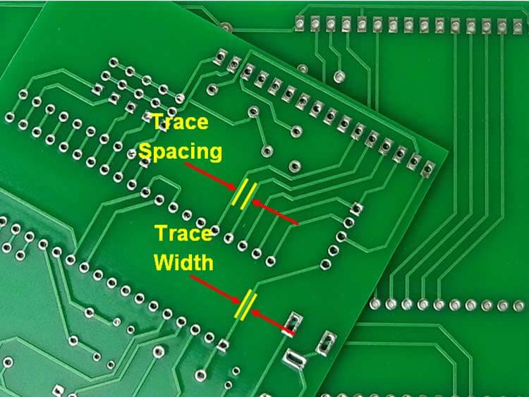
1. Trace Width and Thickness:
Widening and thickening traces are essential for handling high currents effectively. Larger trace widths reduce resistance, minimizing voltage drops and power losses. Calculate trace widths based on current density and allowable temperature rise to ensure optimal performance and reliability.
2. Minimizing Trace Length:
Keep trace lengths as short as possible to reduce resistive losses and minimize voltage drops. Avoid unnecessary detours and use direct routing paths between components to optimize signal integrity and power distribution.
3. Plane Utilization:
Utilize large copper planes as power and ground planes to enhance current distribution and heat dissipation. Ground planes provide a low impedance return path for high currents, while power planes deliver stable power distribution. Ensure sufficient clearance and spacing between planes to prevent unintended shorts.
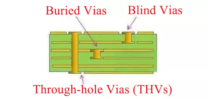
4. Proper Via Selection:
Use vias with adequate size and plating thickness to handle high currents efficiently. Choose via types that can accommodate the required current carrying capacity and ensure proper thermal management. Distribute vias evenly to minimize current density variations and thermal hotspots.
5. Component Placement:
Strategically place high current components close together to minimize trace lengths and routing complexities. Group components with similar functions to streamline layout and reduce impedance mismatches. Consider the proximity to heat sinks and thermal vias when positioning components to optimize thermal performance.
Thermal Management Strategies
As said above, the most important thing in PCB design for high current is managing heat.
So here are some thermal management strategies you can apply for an effective PCB design:
- Use heat sinks to draw heat away from power components and improve thermal conductivity.
- Ensure adequate airflow within the PCB assembly to facilitate heat dissipation and prevent overheating.
- Consider using multilayer PCBs with internal thermal planes for improved heat spreading and dissipation.
By incorporating these layout practices into your high current PCB design, you can enhance reliability, performance, and efficiency while mitigating potential issues associated with high currents.
Conclusion
So that’s how you can design PCBs for high currents. All you have to do is apply these effective layout practices, select components wisely, and implement robust thermal management strategies.
By following these guidelines, you can create high-current PCBs that are reliable, efficient, and capable of meeting the demands of your application.