
Shielded PCBs are crucial in this highly electronics-dense world to safeguard sensitive components from electromagnetic and radio frequency interference. Various performance issues are the result of these interferences.
Signal integrity improves, noise is reduced, and electromagnetic compatibility (EMC) standards are met. This article will explain the shielded PCBs and the various shielded PCBs capable of doing so. Additionally, it outlines the purpose, benefits, and steps involved in designing shielded PCBs.
Purpose of Shielded PCBs
Shielded PCBs are designed to protect electronic components against EMI and RFI. These types of interference disrupt the smooth functioning of the device through malfunctions, data loss, and more. Thus, shielded PCBs guarantee that your devices operate dependably even in high electromagnetic noise environments, such as an industrial setting or a dense recording studio.
Benefits of Shielded PCBs
Shielded PCBs have immense advantages for modern electronic devices. Firstly, the integrity of signals that are transmitted without noise. It implies that the critical components are sufficiently protected to ensure that the noise level is a minimal disturbance. Secondly, shielded PCBs facilitate emission control, ensuring that devices are EMC-compliant. Therefore, devices operate independently, and their compliance is certified.
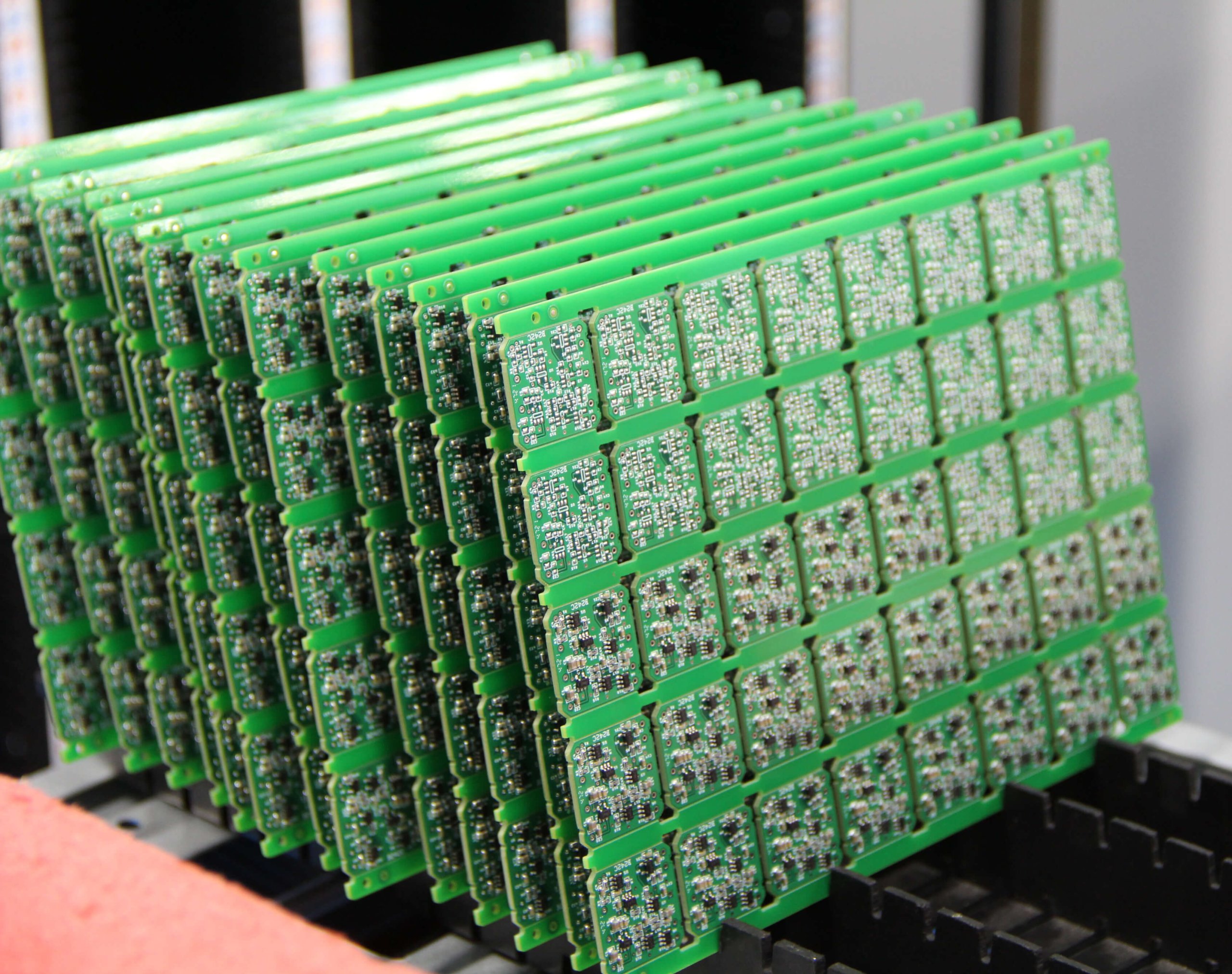
Types Of Shielded PCBs
There are many types of shielded PCBs, each made to meet a particular need for shielding. Knowing these types can make selecting the ideal solution for your application easier.
- Faraday Cages: These enclosures fully surround the PCB, ensuring its protection from any EMI and RFI from all sides. They are made of conductive materials which block out the external electric fields. However, they are recommended for areas with the highest electromagnetic noise.
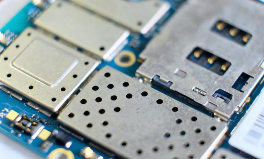
- Metal Enclosures: These are boxes made of a durable material such as aluminium or steel that contain the PCB. Most commonly used enclosures in the industrial and commercial fields have a balance between price and shield.
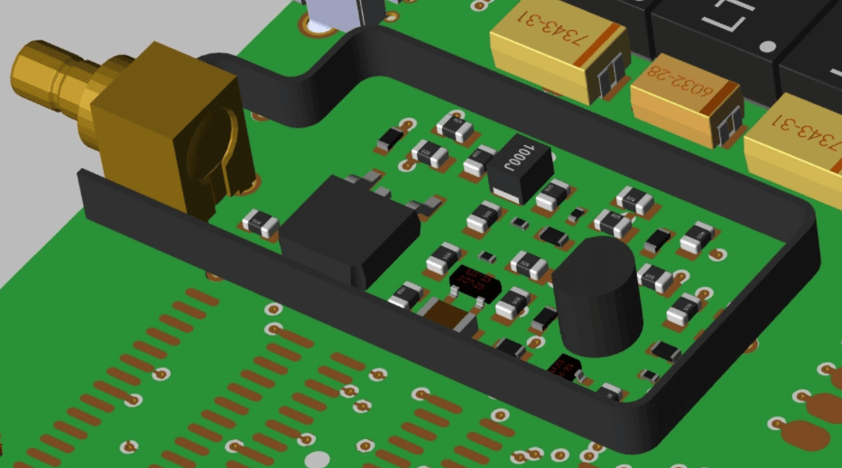
- PCB-Level Shielding: This involves implementing a certain amount of shielding materials directly on the PCB through conductive coatings, layers, or embedding. It is used in designs with a little breathing room, where all relevant aspects are compressed, but the requirement remains specific.
Shielded PCB Design Process
Designing a shielded printed circuit board (PCB) requires several crucial processes to provide good protection against electromagnetic interference (EMI) and radio frequency interference (RFI). Let’s walk you through the procedure.
1. Defining EMI/RFI Requirements
Identifying your device’s EMI/RFI needs is the first step in designing a shielded PCB. Important things to think about are as follows:
- Frequency Range: Point out the frequencies you want your PCB to be protected from.
- Emission Limits: Stick to the emission limits as recommended for market compatibility and legal suitability by bodies like the FCC and CE marking;
- Susceptibility Levels:When considering shielding methods, you must prioritise the system’s most vulnerable parts to EMI, in addition to cost and effectiveness.
2. Shielding Material Selection
Shield design is, in large part, dependent on selecting the proper materials to use. Important factors when picking shielding materials include:
- Conductivity: Copper and aluminium are good choices, as they conduct effectively.
- Thickness: The material’s ability to block harmful interference is directly proportional to its thickness. In General, the thicker, the better.
Expense: Maintain a balance between budgetary restrictions and performance. Although high-performance materials are excellent, they must also be reasonably priced for your application.
3. PCB Layout
Your shielded PCB layout design is a significant factor in the efficiency of your shield. Critical components should be placed within the high-protection regions where the shield absorbs most incoming signals. A solid ground plane is necessary since it acts as a signal return path and lowers noise.
A good ground plane will decrease the loop area and EMI noise. Signal traces must be as short as feasible and as far as possible from any EMI sources, which will improve their signal integrity and lower noise coupling. Success with effective shielding is highly reliant on a good PCB layout.
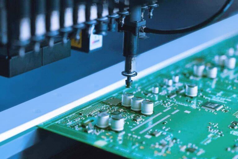
4. Shielding Implementation
There are several ways by which we can achieve shielding implementation:
- Metal Enclosures:For complete robustness, enclose the PCB in a metal box to protect against external interference. Metal enclosures are best for applications that demand the topmost level of protection.
- Conductive Vias:Conductive vias connect the ground plane to the shield to thoroughly shield the areas. They are used to maintain a shield in critical sections and encapsulate areas.
- Conductive Ink:When a shield layer is required on the PCB’s surface, we can use conductive ink for localised shielding. It does not require external support and can be built directly on the PLLC.
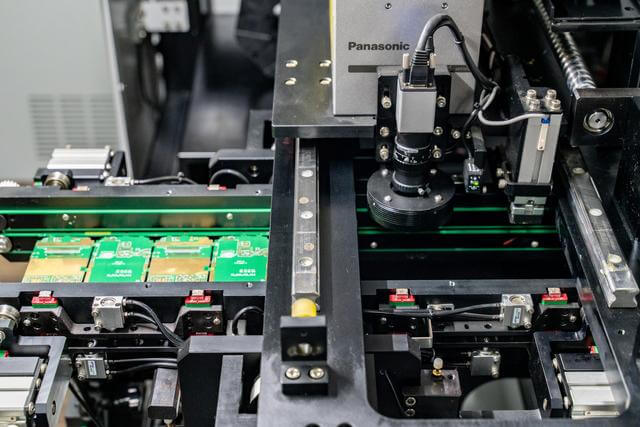
5. Simulation and Analysis
The simulation tool helps you see if your design meets the shielding requirements and whether you will likely encounter other EMI/RFI issues. Electromagnetic simulation software can even tell you what the attenuation of your design will be before you finally take the first step to build it. This gives you prior information on whether your design would meet your specific EMI/RFI requirement or new redesigns.
Common Challenges And Considerations
Several challenges must be addressed when designing a shielded PCB. It is recommended that you address this.
- Shielding Effectiveness:Use appropriate materials and techniques to ensure your shield design blocks EMI/RFI across the necessary frequency spectrum. Testing and modifications should be repeated to achieve the required protection.
- Signal Integrity:Ensure your signal traces have good signal integrity routing and placement by keeping them short and away from interference sources. Use differential pair routing and controlled impedance tracks to ensure a well-designed ground plane to reduce noise.
- Heat Dissipation:During the PCB design, ensure proper ventilation and airflow pathways to prevent the systems from overheating. Use heat sinks, thermal vias, or heat spreaders. Active-cooling alternatives, such as fans or liquid cooling, should be matched with options.
Conclusion
Designing a shield to shield a high-EMI environment is critical for developing a device that performs properly and reliably. By learning the applications, materials, and usefulness of a shielding PCB and applying a structured PCB design process, you can shield key components, increase the operating performance, and comply with EMC.