


Are you struggling with impedance complexities in PCB design? Yes, knowing impedance and being able to calculate it is very important to make sure your printed circuit board is going to have smooth signal transmission.
But do not worry, in this article will walk you through a step-by-step process of determining impedance in PCB design. By the time you finish, you will know what you need in order to manage impedance in your PCB designs.
Well then, let’s get into it.
What is Impedance in PCB Design
Before getting straight to the different methods of calculating impedance in PCB design, it’s essential to first know the basics.
Impedance in PCB design is the opposition to AC passing through an electrical circuit. It has two components: resistance, which is the real part of impedance, caused by the material of the conductor; and reactance, which is the imaginary part of impedance caused by capacitance and inductance.
In simpler terms, impedance is a hindrance to signals that would otherwise flow smoothly through the PCB traces. It’s more like resistance in water when it goes through a narrow pipe: the higher the impedance, the higher the resistance the signal faces, which can lead to degradation or distortion of the signal.
Impedance is well understood to be very important because it, among many others, directly affects signal integrity in high-speed and high-frequency applications. Controlled impedance is part of the reason for this importance.
Let’s further discuss this in detail.
Significance of Maintaining Controlled Impedance
Controlled Impedance PCB Design is critical, particularly in the realm of high-speed, where the least deviation can cause a great problem in signal integrity.
Let us now see why this controlled impedance is important.
- Reducing Signal Degradation: Moving across PCB traces, high-speed signals fall prey to different types of signal degradation, like attenuation, crosstalk, and ringing. Problems caused by these factors are minimized with controlled impedance, which maintains the signal’s integrity along the entire path of transmission.
- Reflection Loss: If the impedances along the path of a signal mismatch, it could be reflected back and thereafter affect the subsequent signals, causing distortion and loss of signal. Impedance control reduces reflection, reducing the possibility of errors or malfunction.
- Improved Signal Quality: In high-speed data transmission or RF communications, where the signal’s integrity is important, controlled impedance is what ensures the proper transmission of the signal. Controlled impedance increases general signal quality and its reliability by reducing distortion and ensuring consistency in signal propagation.
- Facilitate predictable design:By controlling the impedance, controlled impedance designs allow prediction of the behavior of the circuit. The designer will be able to perform the calculation and maintain impedance values with confidence, thus enabling the optimization of the circuit without such unwanted surprises during testing or deployment.
So let’s now describe a few important points that come into play in determining trace impedance in PCB design.
Factors Influencing Trace Impedance
Important factors directly affecting the trace impedance:
- Trace width and thickness
The width and thickness of traces in a PCB are significant. Wide and thick traces make signals flow easily without much impedance. Where the traces are narrow or thin, signals can hardly move and thus are associated with high impedance.
Designers are to pick the right size traces that will be at ease for a signal flow in order to avoid problems.
- Dielectric constant of substrate material
PCB material has a bearing on how fast signals will travel. When the material has a high dielectric constant, it tends to slow down signals, translating to a higher impedance.
Choosing PCB materials with the right properties is important in order to ensure that one has control over impedance and that the signals continue to move well.
- Distance to reference planes
The closer the trace is to other parts, such as ground or power planes, the lower its impedance, since the signals can travel faster. Designers need to ensure that there is always uniform space from trace to other parts to be able to maintain impedance at the right levels and also avoid signal problems.
- The impact of layer stack and ground planes
More importantly, arrangement inside the PCB and the existing ground planes are two major factors. Ground planes act like fast lanes of signals, where the impedance and interference will be quite lower.
So, right layer setup and placing ground planes in a good position will keep impedance under control and signals clean.
- Differential impedance considerations
Some traces carry differential signals that travel in pairs, meaning that one is the opposite charge of the other. Ensuring that these pairs are balanced is vitally important for the integrity of the signal.
Designers balance the impedance between these pairs by using special tools to reduce noise and keep the signals strong. This is what ensures that signals move around electronic systems in a reliable and smooth manner.
A systematic understanding of and control over these parameters play an important role in achieving reliable signal transmission and reducing loss of signal integrity in high-speed electronic systems.
Now you know the basics of impedance in PCB design, it’s time to discuss how you can calculate it using different methods.
Methods for Calculating Trace Impedance
There are 3 different methods you can use to calculate impedance in PCB design.
Let’s discuss them in detail.
1.) Manual Calculations
Manual calculations involve using mathematical formulas to determine trace impedance based on trace geometry and material properties. These formulas typically consider parameters such as trace width, thickness, dielectric constant of the substrate material, and distance to reference planes.
While manual calculations provide insight into the theoretical principles behind impedance calculation, they can be complex and time-consuming, especially for intricate PCB designs.
Additionally, manual calculations may overlook factors like skin effect and frequency dependence, leading to less accurate results compared to other methods.
Here’s a step-by-step guide to manually calculate the impedance of a PCB trace:
Step #1: Identify Trace Parameters:
You need to know the following parameters:
- Trace width (W):The width of the trace.
- Trace thickness (T): The thickness of the trace.
- Copper weight: Usually specified in ounces per square foot (oz/ft^2).
- Dielectric constant (εᵣ): The relative permittivity of the substrate material.
Step #2: Determine Trace Geometry:
Calculate the cross-sectional area (A) of the trace. For a rectangular trace, this is simply the product of width and thickness (A = W * T).
Step #3: Calculate Effective Dielectric Constant:
The effective dielectric constant (εᵣeff) takes into account the influence of the dielectric material on the trace. This can be calculated using approximate formulas or by using specialized software.
Step #4: Compute Impedance:
Use a suitable formula or online calculator to compute the impedance. For microstrip traces (traces on top of the dielectric layer with ground plane beneath), the approximate formula is:
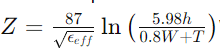
Where:
- Z is the impedance in ohms.
- εeff is the effective dielectric constant.
- h is the height from trace to ground plane (usually the thickness of the dielectric layer).
- W is the trace width.
- T is the trace thickness.
Step #5: Check the Result:
Ensure that the calculated impedance meets your design requirements. If not, adjust trace parameters or consider using impedance-controlled PCB design techniques.
Remember, while manual calculations are educational and can provide rough estimates, for precise impedance control, especially in high-speed digital designs, it’s recommended to use specialized PCB design software or online calculators.
These tools consider additional factors and provide more accurate results.
2.) Using PCB Design Software
Using PCB design software is a more efficient and accurate way to calculate and manage impedance in your PCB designs, especially for complex layouts and high-speed designs.
Here’s how you can use PCB design software for impedance calculations:
1.Select Design Software:
Choose a PCB design software that offers impedance calculation and analysis capabilities. Popular options include:
2.Design Trace:
Create or import your PCB layout into the software. Define the trace geometry, including width, thickness, and layer information.
3.Define Material Properties:
Specify the dielectric material properties, such as the dielectric constant (εᵣ) and thickness, for each layer of the PCB stackup. The software may have predefined material libraries for common substrates or allow you to define custom materials.
4.Impedance Calculator Tool:
Most PCB design software provides built-in impedance calculator tools. These tools allow you to input the trace parameters and automatically calculate the impedance based on the chosen stackup and dielectric properties.
5.Verify Impedance:
After calculating impedance, the software typically allows you to visualize the impedance profile along the trace or perform signal integrity analysis to ensure that the impedance meets your design requirements. You can also simulate signal behavior under different conditions to verify signal integrity.
Using PCB design software streamlines the impedance calculation process, improves accuracy, and allows for comprehensive analysis of signal integrity, making it an essential tool for modern PCB design engineers.
3.) Utilizing Online Impedance Calculators
Online impedance calculators are convenient tools for quickly calculating the impedance of PCB traces without the need for specialized software.
Here’s how you can utilize them:
There are several online impedance calculators available, so choose one from a reputable source.
Some popular options include:
- iCalculator Impedance Calculator:
- AZCalculator Electrical Impedance Calculator:
- Omnicalculator RLC Impedance Calculator:
- Math for Engineers Parallel Impedance Calculator:
Just browse any of these online impedance calculators to calculate impedance in your PCB design within a few seconds.
Online impedance calculators are user-friendly tools that can help streamline the impedance calculation process and ensure the integrity of your PCB designs.
However, it’s essential to understand the underlying principles and limitations of these calculators to interpret the results accurately.
Conclusion
In conclusion, understanding and figuring out impedance in PCB design are really important for making sure signals move smoothly in printed circuit boards.
By knowing the basics of impedance and using different methods to calculate it, designers can deal with impedance problems and make sure signals work well in their PCB designs.