Do you have signal integrity issues with your PCB designs, or maybe you just want to avoid signal reflection for better performance and reliability of your circuit? Signal reflection may lead to signal distortion, data errors, or even system instability, due to impedance mismatches and transmission line effects.
But that shouldn’t be a concern because this article is at your service. Let’s take you through the basic reflections of signals, their effects, and how you could use an efficient method to solve these effects reflected by signals.
At the end, you will know how to design a printed circuit board that shall facilitate signal reflection to a minimum, and thus your circuit will function smoothly.
So, let’s get started.
Importance of Signal Integrity in PCBs
Signal Integrity, hence, refers to the quality of electrical signals traveling on a PCB. Signal integrity is one very important aspect in PCB design since it assures that transmission is done inaccurately and effectively, hence without distortion or loss of signals.
This signal integrity is to be maintained properly because of the importance of circuit performance, more so in high-speed applications with reference to both digital and analog techniques.
Signal reflection occurs when a signal traveling through a PCB trace encounters an impedance mismatch, causing a portion of the signal to be reflected back toward the source. This can be compared to how a wave reflects off a surface or how a ball bounces back when it hits a wall.
In fact, such reflections can distort the original signal in a PCB, thus creating following effects:
1.Impedance Mismatch
This would be where trace impedance does not match either the source or load impedance and, in so doing, invites reflections. The disparity can arise in many ways, be it a variation in trace width, change in dielectric material, or improper termination.
2.Transmission Line Effects
It can occur at very high-frequency applications when PCB traces show characters of the transmission line. If not well designed, the mentioned traces can cause signal reflections.
3.Other Negative Effects
- Signal Distortion:The signals possibly reflected back can join the original transmitted signal. It often—in elevated rise and fall times, besides prefabrication of ringing or overshoot and undershoot.
- Data Errors:Distortion of the signal might lead to data distortion and cause transmission errors that lower the reliability of the whole system.
- System Instability: A further reflection of the signal may cause crosstalk in which signals from two closely located traces interface with each other and adversely affect the system’s stability, causing it to eventually fail.
Understanding and mitigating signal reflection is essential for designing robust PCBs that perform reliably in real-world applications.
Understanding Signal Reflection
Signal reflection is a very important phenomenon in electronics and communications, notably for important items like high-speed signal on transmission lines, such as PCB tracks.
Let’s break down the basic concepts behind signal reflection using simple analogies and explanations.
Imagine you throw a stone into a calm pond. The water will be displaced and form ripples which, in turn, spread. The ripples carry on when they hit an obstacle, like the edge of the pool or another rock, and then recoil. This is reflection.
Now consider bouncing the ball on a wall: the ball is thrown against the wall and comes back at the thrower. The harder the wall is, the faster the ball is going to come back. If the wall is soft or lumpy, then chances are that the ball will come back at a slower velocity or at an angle. Clearly, what the wall consists of helps to determine how the ball bounces back.
Signal Reflection on Transmission Lines (PCB Traces)
In electronics, a signal traveling along a transmission line (like a PCB trace) can hit changes in impedance, such as connectors or bends. These changes can cause part of the signal to reflect back to the source, similar to water waves hitting an obstacle or a ball bouncing off a wall.
Voltage and Current on a Transmission Line
The signal wave is represented by voltage and current coexisting on a transmission line. When the wave reaches the level of impedance discontinuity and it reflects back, a portion of the signal wave may cause interference or signal problems, especially in high-density circuits.
To get a better understanding, consider a transmission line with a load at the termination end. If it is matched to the line’s impedance, then the signal is treated exactly as the way it should and no reflected signal is present.
If a mismatch exists, then part of the signal reflects back, forming along that line of transmission a standing wave pattern.
Characteristic Impedance
The characteristic impedance (Z0) of a transmission line is a property that defines how signals travel along the line. It depends on the line’s size, materials, and the signal’s frequency. It’s like the line’s natural resistance to signal flow.
When a signal travels along a line with a constant characteristic impedance and hits a load with the same impedance, there is no reflection. The load perfectly matches the line’s resistance, so the signal passes through smoothly.
But if the load impedance is different from the line’s impedance, part of the signal reflects back. If the load is much higher or lower than the characteristic impedance, the reflection is stronger.
Impact of Signal Reflection
Signal reflection can negatively affect the performance of a printed circuit board (PCB). Here are the main problems it can cause:
- Increased Signal Rise/Fall Times and Ringing (Overshoot/Undershoot)
When a signal reflects back and forth on a PCB trace, it can slow down the rise and fall times. This means the signal takes longer to switch from low to high or high to low, which can cause timing issues.
Ringing happens when the reflected signal adds to the original signal, causing it to overshoot (go higher than intended) or undershoot (go lower than intended). This can create oscillations that distort the signal, making it hard to read correctly.
- Data Corruption and Transmission Errors
Reflected signals can interfere with the original signal, leading to data corruption. This is especially bad in high-speed circuits, where timing is critical. Distorted signals can result in transmission errors, where the data received is not the same as the data sent. This can cause devices or systems to malfunction.
- Crosstalk (Unwanted Signal Coupling) Between Adjacent Traces
Crosstalk is when signals on nearby PCB traces interfere with each other. Reflections can make crosstalk worse by adding extra noise. When a reflected signal affects a nearby trace, it can cause voltage changes that interfere with the signal on that trace, leading to data errors and reduced signal quality.
- System Instability and Potential Malfunctions
Signal reflections can cause system instability. Reflections create unexpected voltage levels or noise, leading to unpredictable system behavior.
This might cause intermittent failures, glitches, or even complete system crashes. In critical applications, like medical devices or aerospace systems, this instability can be very dangerous.
Mitigating Signal Reflection (Solutions)
To ensure reliable performance of PCBs, it’s essential to mitigate signal reflection.
Here are practical solutions with clear explanations.
Impedance Matching
Matching the trace impedance to the source and load impedances is crucial to prevent signal reflections. When the impedances are mismatched, part of the signal reflects back, causing interference and signal integrity issues.
Methods for Calculating Trace Impedance
- Online Calculators: Many online tools allow you to input trace dimensions, PCB stack-up, and dielectric properties to calculate impedance.
- Design Tools: Software like Altium Designer or Cadence includes impedance calculators to help design traces with the correct impedance.
Techniques for Adjusting Trace Width, Spacing, and Dielectric Material
- Trace Width: Changing the trace width affects the impedance. Wider traces reduce impedance, while narrower traces increase it.
- Spacing: The spacing between traces and ground planes can also affect impedance. Closer spacing reduces impedance.
- Dielectric Material: The material between the trace and the ground plane influences impedance. Different materials have different dielectric constants.
Termination Techniques
Termination techniques help absorb reflected energy and match impedances to prevent reflections.
Here are some common methods:
Series Termination
- Description: A resistor is placed in series with the signal source.
- Application: Effective for point-to-point connections where the load impedance is high.
Parallel Termination
- Description: A resistor is placed between the signal line and ground at the load.
- Application: Useful for matching the impedance at the load end.
Thevenin Termination
- Description: Combines resistors to match impedance and provide a stable voltage level.
- Application: Common in systems requiring precise voltage levels.
Choosing Appropriate Termination Resistors
- Signal Characteristics: The resistor values should be chosen based on the trace impedance and the characteristics of the signal (frequency, voltage levels, etc.).
- Example: For a trace with 50 ohms impedance, a series resistor of 50 ohms or a parallel resistor of 50 ohms to ground can be used.
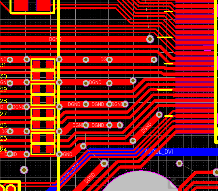
PCB Layout Guidelines
Controlled Trace Length
- Design Rule: Keep trace lengths as short as possible to minimize reflections and maintain signal integrity.
- Justification: Shorter traces reduce the chance of signal degradation and timing issues.
Avoiding Sharp Bends
- Design Rule: Use gentle curves or 45-degree angles instead of sharp 90-degree bends.
- Justification: Sharp bends can cause impedance discontinuities, leading to reflections
Proper Component Placement
- Design Rule: Place components to minimize trace lengths and avoid crossing signal paths.
- Justification: Shorter, direct connections reduce reflections and crosstalk.
Differential Signal Routing Techniques
- Design Rule: Use differential pairs for high-speed signals, keeping the pairs close together and of equal length.
- Justification: Differential pairs help cancel out noise and maintain signal integrity.
Final Words
Signal reflection can significantly affect how well your PCB works. Understanding how it happens and its negative effects is key to improving your circuit’s reliability.
By matching trace impedance correctly, using the right termination methods, and following good PCB layout rules, you can reduce signal reflections. These steps help ensure your circuits work smoothly, with fewer errors and better performance.
Implementing these solutions will improve signal integrity and stability in your PCB designs, making them more reliable for their intended applications.


