Are you facing fanout violation issues in your PCB layout? They can cost you in signal weakening and potential trace interference.
Do not worry, though. This article is going to help you understand the roots of these violations and show you simple ways to fix them. We are going to discuss easy strategies that will help in keeping your PCB design on track.
So, let’s begin.
Understanding Fanout in PCB Layout

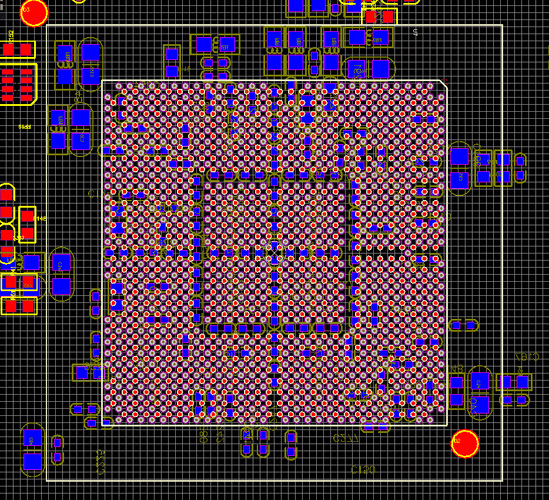
Fanout is the process of sending a single signal from a driver, like a gate or buffer, to several receiving circuits, such as logic gates or other components. This corresponds, in the case of a PCB design, to routing a signal in a manner that it can reach several points on the board.
Proper fanout is the thing that will sustain the strength and integrity of your PCB signals. In case, fanout has not been properly done, then you will have a weak signal that might not be able to reach all parts of the board effectively.
This will result in slower signal responses and timing problems. This also can lead to the situation of crosstalk, where the signals are said to interfere with each other. It often disturbs the performance of a circuit. Good fanout helps in avoiding these problems and keeps your PCB in good health.
Now let’s discuss the fanout violations in PCB layout in detail.
Fanout Violations in PCB Layout
Fanout violations happen when too many loads are connected to a single driver, exceeding its ability to send a strong, clean signal to all destinations.
When the driver has to handle more connections than it can manage effectively, it struggles to maintain signal quality. This often leads to problems in the PCB layout.
Consequences:
- Signal Attenuation: As the signal travels through the fanout traces, it can lose strength, making it harder for the signal to reach its destination clearly. This weakening can cause issues with the overall performance of your circuit.
- Increased Rise and Fall Times: If care is not exercised, fanout can bring slowdowns in the transition of the signal. It indicates how fast the signal ought to turn either high or low. Delays in these will introduce timing problems, eventually affecting the performance of your circuit.
- Crosstalk:Excessive fanout can cause signals to interfere with each other. This undesired coupling of signals between nearby traces can lead to crosstalk, which can disrupt the functioning of your circuit and reduce its reliability.
Now you know the consequences of fanout violations in PCB layout, it’s time to learn how you can avoid them.
Strategies to Avoid Fanout Violations
Here’s how you can avoid fanout violations:
Fanout Calculation:
To prevent fanout violations, start by calculating the fanout requirements. This involves considering several factors:
- Driver Output Current Capability:This is the current the driver can supply to connected loads; make sure the driver current capability of this device meets the total current supplied on all connections.
- Load Capacitance:Notice the capacitance of each circuit received. Higher capacitance can put more strain on the driver, so it’s important to account for this in your calculations.
- Trace Length and Impedance:The traces’ length should be measured all the way through, along with their impedance. Longer traces and bigger impedance result in worse changing signal quality, so they must be optimized against your design.
Buffering:
One practical method of dealing with higher fan-out without degrading the quality of the signal is to use buffers. The role that buffers will play in this is as an intermediate to beef up the strength of the signal for it to then effectively reach destinations, many of them at a time.
That will help you increase the number of connections while keeping the signal strong and clean.
Trace Impedance Control:
Keeping trace impedance consistent helps to avoid signal problems. Reflections and crosstalk can be created in the signal when there are changes in impedance along a fan-out path.
You can do this by adjusting trace widths as needed and then using controlled impedance materials to keep the same impedance on all traces.
Star Routing:
Star routing is a technique where each receiving circuit has its own dedicated trace from the driver.
This method helps reduce the chances of crosstalk and signal interference by ensuring that each signal path is isolated from others. It’s an effective way to manage fanout in densely packed designs.
Design Considerations
Here are some design considerations that will help you prevent fanout violations while designing:
- Component Placement:
Careful placement of components at the very least reduces fanout problems. Keeping components close to one another will help in keeping trace lengths short, which in turn reduces fanout.
This will help the signals to travel more efficiently and stay strong and clear. Try to locate the component, keeping the paths of the signals as straight as possible.
- Power and Grounding:
Good power and grounding are conducive to the sustainment of the performance for your PCBs. Proper power distribution will ensure each component is fed a stable voltage, and good grounding will minimize noise and issues with the signals.
If the design has a high fanout, then poor power and grounding may only increase these problems. In such designs, your PCB should be designed with good planes of power and ground for reliable support under high fan-out conditions and quality signals.
Final Thoughts
Avoiding fanout violations is key to keeping your PCB design reliable and efficient. By understanding fanout, calculating requirements, and using strategies like buffering and trace impedance control, you can prevent common problems.


