Gerber file errors cause major singularities in PCB manufacturing. How many times have you experienced added delays or costs because of errors in your Gerber files? This could be due to missing layers or wrong sizes, among other things, which cause problems when it comes to time for production.
But don’t worry as this guide will help you understand and avoid these common problems. With easy tips and solutions, you will keep your Gerber files error-free and your project on track.
So, let’s get started.
Understanding Gerber Files
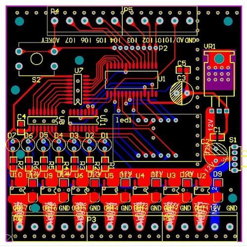
Gerber files are the standard way to transfer the details of a PCB design to a fabrication house. It translates your design elements into detailed instructions that provide guidance for the processes of conduction.
Basically they are a blueprint that details everything from the layout of the board to the placing of components to where the drill holes will be. Each file represents yet another layer of the PCB, for example the copper traces, the solder mask, and the silkscreen.
These files enable fabrication houses to manufacture the exact copy of your design in a PCB. So then, by following these files, such a house can make a PCB that will help realize your described product and see it function exactly whatever it was set forth to do. Suitable understanding and preparation of Gerber files are important for a smooth manufacturing process.
Now let’s discuss different types of errors in Gerber files that you might face.
Types of Errors in Gerber Files
Errors in Gerber files can cause big problems in PCB manufacturing. Here’s a simple guide to common mistakes and how to avoid them:
1. Data Errors
- Missing or Incomplete Files:Make sure you provide all the necessary Gerber files, like the board outline, drill data, and soldermask definitions. Each file represents a different part of the PCB, so don’t leave any out.
- Incorrect Units:Check that your design units (millimeters or inches) match what the manufacturer expects. Using the wrong units can lead to sizing and placement errors.
- File Naming Conventions and Format:Please use clear and consistent file naming to avoid confusion and delays. File format is also important. Please use common Gerber file formats, such as 274X, RS-274G, etc.
2. Design Rule Violations (DRVs)
- Trace and Clearance Issues:Ensure traces are not too thin or clearances between features are not too narrow. Either condition might cause shorts or weak connections.
- Drill Size Discrepancies:Make sure drill sizes in your Gerber files align with the board’s specifications; mismatched sizes can raise problems with component placement and vias.
- Incorrect Layer Stackup:Ensure that the layer sequence is correct; the wrong stackup may produce the misalignment of vias or connections on the unfinished PCB file.
3. Artwork Errors
- Aperture Errors:Confirm aperture settings are correct; inappropriate settings allow vias or pads to have the wrong shapes.
- Negative Images:Some manufacturers don’t support negative images although it’s usually best to work with positive images for compatibility reasons.
- Flash and Polygonal Errors:Look out for excess copper—termed as flash or polygon errors—reaching out to connect and short inadvertently.
You can find these common errors early on to help ensure the sleekness of your PCB manufacturing process.
Preventing Gerber File Errors
Here are a few practical tips to help you prevent Gerber files errors:
1. Design for Manufacturability (DFM)
Designing your PCB with manufacturability in mind from the start can save you a lot of trouble. Stick to standard industry practice and conform to the specific DFM rules of your manufacturer.
It means designing with the manufacturing process in mind, in such a way that the final PCB will be built precisely as intended without any hitches.
2. Use Design Rule Checking (DRC)
Make use of DRC tools in your PCB design environment, which, in practice, would give you the freedom of being able to find potential design rule violation mistakes and pinpoint them prior to generating your Gerber files.
By catching issues early, you can prevent errors that might otherwise cause problems during manufacturing.
These will enable you to create error-free Gerber files and ensure a smoother PCB manufacturing process.
Conclusion
Avoiding errors in Gerber files is key to a smooth PCB manufacturing process. By making sure your files are complete and correctly formatted, checking for design rule violations, and using DRC tools, you can prevent common problems.
Designing with manufacturability in mind also helps ensure your PCB meets all specifications. With these steps, you’ll reduce the chances of delays and costly mistakes, making your project run more smoothly.

