


Have you just discovered PCB Silkscreen and wondered how PCB manufacturers create it? Look no further, as this guide is here to help you.
For many people, it may seem daunting to understand PCB silkscreening, especially for newbies who are fresh to the world of PCB fabrication. But worry not; this guide is here to help demystify the process.
Whether you are reading this guide as a seasoned professional needing a refresher or a beginner entering the world of printed circuit boards, this will definately help you.
So let’s get started.
Understanding PCB Silkscreen
In simple words, PCB silkscreen is text, symbols, and graphics overlaid on a printed circuit board. Its primary purpose is to provide critical identification and guidance throughout assembly, testing, and maintenance.
The silkscreen helps a technician properly mount the PCB with its components marked out, together with their placements and even, to some extent, their orientation, hence reducing errors in the processes and ensuring the correct functioning.
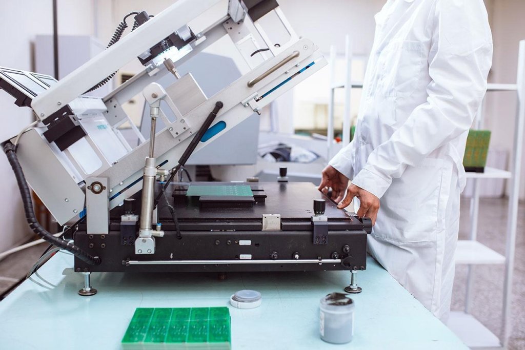
In the silkscreening process, PCB manufacturers play an important role. Utilizing specialized equipment and techniques, they print the silkscreen layer onto the PCB surface, aiming for high-quality, durable prints that meet industry standards.
Now let’s discuss the PCB Silkscreening process in detail.
The PCB Silkscreening Process:
The silkscreening process of the PCB consists of a number of distinct stages:
1.Silkscreen Artwork Setup:
Creation of the digital file, or layout, for the silkscreen legend containing text, symbols, and markings in the proper design software.
2.Stencil Making:
To create stencils according to the silkscreen artwork using the photoresist film and photolithographic process. This stencil will then indicate the areas where the ink will be applied to the PCB.
3.Screen Preparation:
The application of a photosensitive emulsion on a mesh screen and then the stencil registration on top of that screen. The screen-stencil combination later gets exposure to UV light, which consequently hardens the emulsion located in spaces exposed through the stencil.
4.Stencil Development:
Rinsing off the emulsion areas that were not exposed, which will leave openings on the stencil itself according to the desired silkscreen pattern. These openings allow ink to pass through and deposit patterns on the PCB surface during printing.
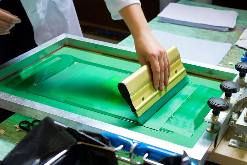
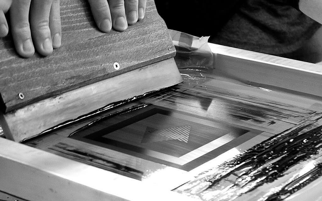
5.Inkjet Printing or Squeegee Printing:
By passing through the openings in the stencil, a thin film of silkscreen ink is transferred to the PCB surface. This can be implemented through either inkjet printing technology or even a squeegee-based method.
6.Curing and Drying:
The applied ink is allowed to dry on the surface of the PCB on its own. Sometimes, a UV curing process is also applied wherein the inks are further made to attach themselves to the board and become challenging in the process.
7.Stencil Cleaning:
Finally, the process of removing any remaining ink from the stencil so that it can be used again without problems in future silkscreening operations.
Some manufacturers may use alternative techniques such as Liquid Photo Imaging (LPI). This is where a liquid photo imageable solder mask is applied to the surface of the PCB, and UV light is used to solidify it via a negative image mask.
In this process, after exposure to the light, the mask is developed to wash out unexposed parts, leaving the intended silkscreen pattern behind. The LPI is known to have finer resolution and is more flexible toward design, but that will be technologically enabled.
Materials Used in PCB Silkscreening
Few of the significant materials used in PCB silkscreening are:
1.Silkscreen Ink:
Silkscreen ink is the main element that prints the text, symbols, and graphics on the surface of the PCB. It is like the “paint” but needs to be developed, especially for the electronics industry.
The color of the selected ink shows a pleasing contrast that can adhere without sublimation in both handling and use of the PCB. Opacity is required to cover up any underlying patterns or markings on the PCB.
The ink is also surface compatible concerning the surface finish of the PCB to attain good adhesion and durability.
2.Stencil Material:
A stencil is a thin sheet with holes that determine where the ink goes on the PCB. Usually, it is made up of stainless steel or polyester. Stainless steel stencils are very precise, meaning they can create very detailed designs accurately.
They work very best with fine-pitch components and complicated patterns. However, it might get costlier.
On the other hand, polyester stencils are cheap and comparatively more flexible than their stainless-steel counterparts; however, they may not be that durable and accurate.
3.Photoresist Film:
Another special kind of material used to make the stencil is photoreactive film. This material is light-sensitive hence its properties are altered when exposed to UV light.
When the UV-exposed movie is treated with an alkali solution, the hardening takes place in the exposed parts, and the rest remains soft; the latter parts are washed off, leaving the stencil pattern.
Dry photo imageable and liquid solder masks are other types of the photoresist film. They are mainly used throughout the PCB manufacturing process and generally have advantages over these two films.
Design Considerations for PCB Silkscreen
When designing PCB silkscreen legends, several key factors contribute to their effectiveness:
- Clarity and Readability:
Appropriate symbol sizes, clear fonts, and proper spacing are all crucial factors. Fonts should be chosen based on legibility, avoiding those that are overly stylized or complex.
The size of symbols needs to be big enough so the user can recognize them, particularly when components have small text or intricate symbols. Proper spacing between elements prevents overcrowding and enhances clarity.
- Placement and Orientation:
Silkscreen elements need to be placed strategically to be easily visible for viewing during design and testing. Components should be labeled in areas where it is easy to reach them and view them without interfering with other circuit traces or components.
Also, as part of best practice, the correct orientation of the board needs to be respected for the placement of symbols and labels to avoid mistakes in assembling during soldering and assist in troubleshooting effectively.
- Durability and Adhesion:
It is essential to choose silkscreen ink and processes that allow the marks to be resistant to soldering and harsh environments in the long term. Of course, the ink should bond securely to the PCB surface and resist fading, smudging, or peeling during soldering, cleaning, and operation.
Most importantly, additional bonding and durability can be improved by using special inks and curing processes for PCBs used in rugged or high-temperature environments.
- Design Standards and Best Practices:
Designing a PCB silkscreen following industry standards and guidelines, like those authored by IPC (Association Connecting Electronics Industries), ensures consistency and reliability.
The IPC recommends text sizes, line widths, spacing, and other design parameters. These are going to preserve legibility and ease manufacturability while bringing down manufacturing costs improving quality, and minimizing errors.
With all these factors in mind during the design process, engineers can create PCB silkscreen legends that are clear, durable, and meet industry standards for the usability and reliability of the final product.
Conclusion
In conclusion, silkscreening in PCB is a very critical process in the creation of printed circuit boards. This helps technicians with clear labeling and marking for component placements and orientations.
With this guide, both newcomers and experienced professionals can gain a better understanding of the PCB silkscreening process and its importance in PCB manufacturing.