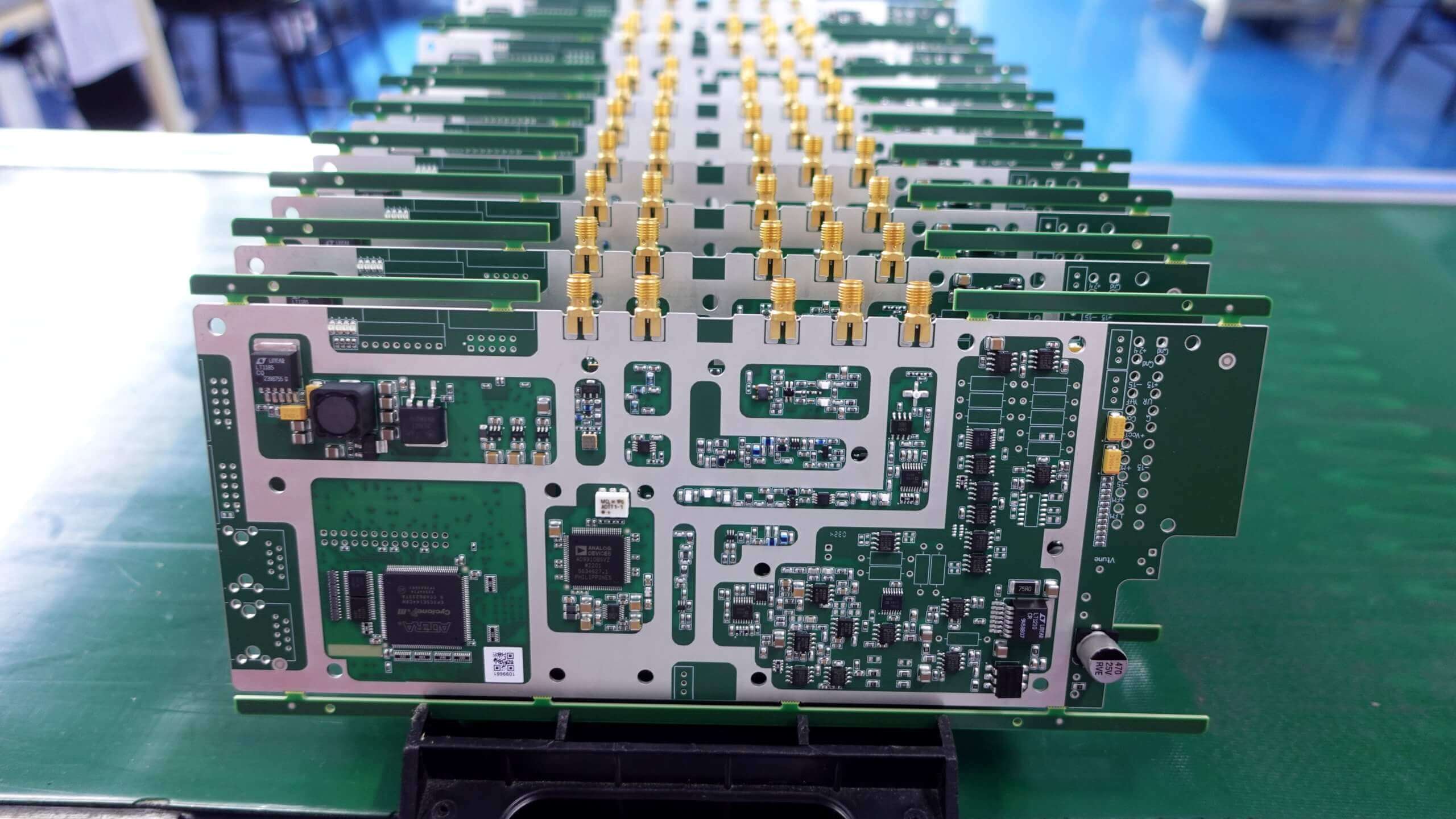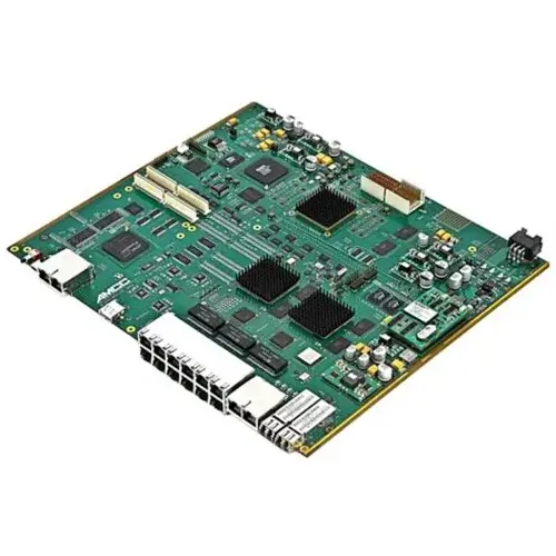
main chipset
A piece of DSP TMS320C13B chip, NVRAM 2M bytes
Two FPGA Lattice LFXP6C chips
DSP chip 2MB FLASH, 8MB SDRAM
technical parameter
32 I/O inputs and 64 I/O outputs
2-way optical isolation RS232
1 RS422 interface and 1 RS485 interface
48-way 16-bit synchronous 200KSPS A/D conversion
One photoelectric isolation CAN interface and one GPS timing
Built-in real-time clock, power monitoring and watchdog, etc.
Support -40~85℃ industrial wide temperature application
circuit diagram
Introduction to PCBA of Digital Image Acquisition and Processing System
The digital image acquisition and processing system PCBA can realize high-speed image acquisition and storage of the camera, compress and serially communicate with the PC to realize the transmission of image data, realize image processing and display on the PC, etc. The PCBA design mode of the digital image acquisition and processing system adopts the hardware acquisition-software processing mode. After the image is sampled and quantized, it is converted into a digital image and input and stored in the frame memory. The image is analyzed by a computer to achieve the desired result. Digital image acquisition and processing system PCBA can be used in video conferencing, security monitoring, traffic charges, industrial inspection, image acquisition and other various image acquisition, processing and analysis fields.
technical parameter
32 I/O inputs and 64 I/O outputs
2-way optical isolation RS232
1 RS422 interface and 1 RS485 interface
48-way 16-bit synchronous 200KSPS A/D conversion
One photoelectric isolation CAN interface and one GPS timing
Built-in real-time clock, power monitoring and watchdog, etc.
Support -40~85℃ industrial wide temperature application

