


Have you ever wondered how to protect your electronic devices from moisture, dust, and extreme temperatures? Well, here is an answer: choose proper PCB potting compounds for the application.
In the market, there are different types of PCB potting compounds available in the market, making it difficult to choose the right one.
But don’t worry as this article is here to help you. By the end of this, you will be confident in selecting the suitable potting compound to hold your electronics safe and in perfect working order.
So, let us begin.
What is PCB Potting
Several environmental factors could make an electronic circuit function abnormally or fully malfunction. Moisture initiates the process of corrosion and the creation of short circuits; dust and other impurities are likely to interrupt the contact of the circuits.
Other factors include vibrations and temperature extremes, which, in addition to mechanical stress and thermal damage, also impact the reliability of electronics.
Therefore, PCB Potting becomes a solution to these problems.
PCB potting is the process whereby electronic components and a printed circuit board are encapsulated in a potting protective material, generally resin or compound. The protective coating or potting compound protects the hostile environment and prevents moisture, dust, vibration, mechanical shock, etc., from entering sensitive components.
In addition, it enhances good thermal conductivity and good electrical insulation, which will make the electronic device work seamlessly and last longer.
Types of PCB Potting Compounds
There are several types of PCB potting compounds in use. Let’s discuss the most common ones:
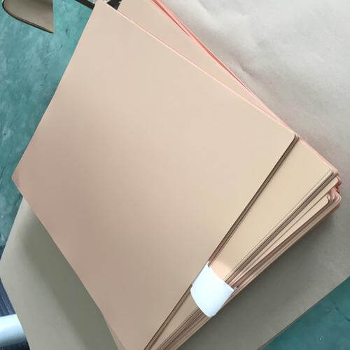
- Epoxy: Epoxy is tough and handles chemicals well, making it suitable for packaging electronic circuits; however, it can crack very easily under heavy impacts.
- Silicone: Silicone is a very flexible and suitable material that works well under high temperatures or in wet conditions. It brings good watertightness but perhaps would not be as resistant to physical stress as epoxy is.
- Polyurethane (PU): The material adheres well on PCBs and has good vibrational absorption—essential to protect machine electronics. It is not affected by chemicals, though it sets up slower than with epoxy or silicone.
Now you know the basics of PCT potting compounds, it’s time to learn how to choose the right one.
Choosing the Right PCB Potting Compound
Here’s how you can choose the right PCB potting compound:
1.Environmental Conditions
Evaluate the specific environmental concerns the PCB will be exposed to, such as humidity, temperature changes, or exposure to chemicals or outdoor elements.
2.Mechanical Strength and Vibration Resistance
Establish the amount of mechanical stress and vibration applied to the PCB. Select a potting compound to provide enough strength and damping capabilities to accommodate these inputs.
3.Thermal Management Requirements
Make sure to consider the circuit thermal conductivity requirements; select a potting compound that should be capable of efficient heat dissipation in order to maintain ideal thermal properties for ensuring that the component does not overheat and that it functions with reliability.
4.Adhesion Properties
Evaluate the adhesion of the potting compound to the PCB and the electronic components. The adhesion has to be vital to maintain the potting’s integrity.
5.Curing Process Compatibility
Check the compatibility of the curing process of the potting compound with your production setup–heat curing, UV light exposure, or moisture curing could be involved.
6.Workability and Safety Considerations
Evaluate the potting compound concerning ease of handling and ease of application during manufacturing. Ensure due consideration has been given to safety because of factors like ventilation and personal protection, both when handling the material and during curing.
By careful assessment of these factors, you can choose the suitable PCB potting compound, which will best serve your application through long-term reliability and environmental guarding.
PCB Potting Process
The PCB potting process can be broken down into a few simple steps:
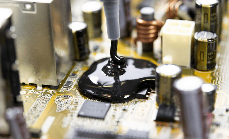
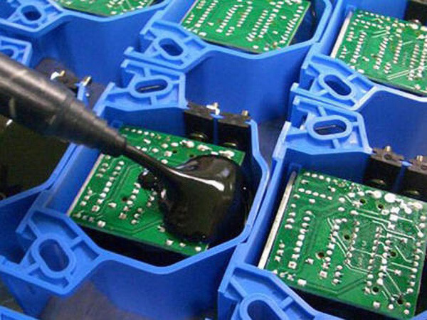
- PCB Cleaning and Preparation: The PCB surface must be very clean before potting to remove dust and oils that could affect adhesion. A rule of thumb is to ensure adequate adhesion of the potting material over the entire PCB.
- Component Masking: Not all components on the PCB, such as sensors or connectors, may work along with potting material. Therefore, these sensitive areas must be masked to shield them from becoming covered or affected by the potting.
- Potting Compound Selection and Preparation: Select the correct potting compound concerning the needs of your application, environmental conditions to be met, and mechanical protection to be provided. Follow the manufacturer’s instructions for mixing or activating the compound to ensure proper consistency and effectiveness.
- Potting Application: Disseminate the potting material uniformly into and all around the design of the PCB through the selected method, whether by uses of pouring or injecting. This will thoroughly coat it to enclose the whole circuit board with a protective barrier.
- Curing: Now allow the potting compound to cure for an adequately long period at the correct temperature according to the stipulated curing instructions from the manufacturer. Correct curing guarantees the proper hardening of the compound and maximum protection.
- Inspection and Testing: After curing, see whether or not the PCB has been properly potted. Test the circuit functionality to ensure that the potting process has not affected electronic performance.
Safety Considerations
Apply these safety precautions to work safely with PCB potting compounds and handle them properly.
- Proper PPE: Proper gloves, safety glasses, and maybe a respirator should always be used to protect yourself from contact with the potting material and any potential fumes.
- Ensure Adequate Ventilation: Work in a well-ventilated place; otherwise, vapor exhalation during the mixing, application, and curing of potting compounds can result in possible fume inhalation.
Uncured Compounds: Handle uncured potting compounds according to the information in this datasheet. Follow recommended procedures to minimize the potential for exposure and prevent any side effects.
Common Problems and Troubleshooting
Here are some common problems that you might face during PCB potting process and troubleshooting techniques to help you:
1. Air Bubbles
Air bubbles can get trapped in the potting material during application, which can affect how well it protects the PCB. To avoid air bubbles:
- Use a vacuum device to remove air from the potting material before applying it.
- Apply the potting compound carefully to minimize air getting trapped.
2. Incomplete Curing
Sometimes, it so happens that the potting material leaves the PCB unhardened. To ensure a complete cure:
- Follow exactly the instructions for curing time and temperature.
- Keep the temperature stable during curing to allow the compound enough time to harden fully.
3. Component Damage
Applying a potting material upon the components can cause spilled and cover/harm sensitive parts of the PCB. The following measures should be taken to avoid this:
- Cover sensitive parts before application of the potting compound.
- Choose a potting compound that does not harm the functional PCB equipment.
Final Words
Choosing the right PCB potting compound is crucial for protecting circuits from moisture, dust, vibrations, and extreme temperatures. Options like epoxy, silicone, and polyurethane offer different strengths.
Follow the PCB potting process carefully, prioritize safety with proper gear and ventilation, and ensure thorough curing for reliable electronics protection.