


Surface Mount Technology (SMT) is an advanced method in modern electronics production. It uses automated machines to place and solder tiny electronic parts directly onto circuit boards. The key advantage of SMT is its ability to quickly pack components densely onto boards using precise equipment, replacing older through-hole technology (THT) that required drilling holes.
What is SMT Assembly?
Surface mount technology (SMT) is a method of producing electronic circuits by directly placing components on the surface of circuit boards.
SMT assembly emerged as an alternative to through-hole mounting in PCB manufacturing, which peaked in the 1970s-1980s. As electronics manufacturing evolved, more efficient and refined processes became essential. SMT assembly was developed precisely to meet this demand.
Advantages of SMT Assembly
Space Efficiency and Miniaturization Breakthroughs
- Achieves 40%-60% volume reduction and 60%-80% weight reduction using miniature components (e.g., 0201, 0402 packages).
- Smartphone motherboards integrate over 200 solder points per cm², supporting high-density wiring in wearables like smartwatches.
- Directly enables the slim trend in consumer electronics.
Full Automation and Efficiency Leap
- Automated production: Placement machines handle 50,000 components/hour, reducing labor costs by 50% compared to THT.
- Improved yield: AOI systems detect defects as small as 0.01mm. Combined with multi-zone reflow soldering, yields rise from 85% (THT) to >99.9%.
- Flexible manufacturing: Intelligent feeder systems enable rapid line changes (e.g., FUJI NXTR placement machines) for small-batch orders.
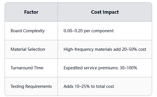
Cost Control and Environmental Benefits
- 30%-50% lower total costs by eliminating drilling processes, material waste, and production time.
- Lead-free compliance: Meets RoHS standards for medical devices and automotive electronics.
- Energy optimization: Automated equipment consumes 20% less power; multi-lane placement machines reduce space/energy usage.
SMT Assembly Process Flow
-
Core Steps
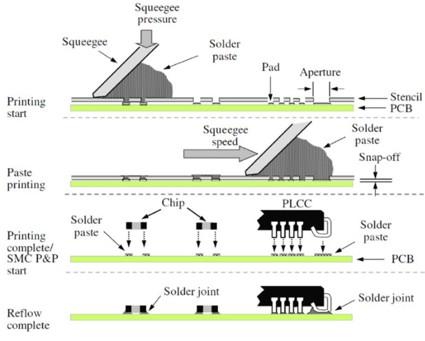
- Solder paste printing: Uses stencils to apply precise solder paste patterns on PCB pads.
- Component placement: High-speed machines position SMDs with micron-level accuracy using vacuum nozzles.
- Reflow soldering: Controlled temperature profiles (preheating, soaking, reflow, cooling) create reliable solder joints.

- Inspection & rework: AOI, X-ray systems detect defects; rework stations address anomalies.
Special Scenarios
- Double-sided assembly: Reflow one side, flip PCB, then use wave soldering or secondary reflow for the other side (temperature control critical).
- Red glue process: Adhesive fixes components before wave soldering, eliminating reflow steps.
SMT Applications
- Consumer Electronics
Smartphones, laptops (e.g., iPhone motherboards with 1,000+ components via double-sided SMT). - Automotive Electronics
Engine ECUs, ADAS systems meeting automotive-grade reliability (-40℃~125℃ operation). - Industrial & Medical
Industrial controllers, MRI equipment achieving <10ppm failure rates. - Aerospace & Defense
Radar/Satcom modules using radiation-hardened SMT components.
SMT vs. THT Technology
Modern SMT trends focus on “ultra-miniaturization + intelligence”:
- 01005 packages and 3D SiP stacking becoming mainstream
- AI-powered AOI systems achieving >99.9% defect recognition
- Critical directions: digital material management (MES) and green manufacturing (halogen-free solder) to meet 5G/AIoT demands.