


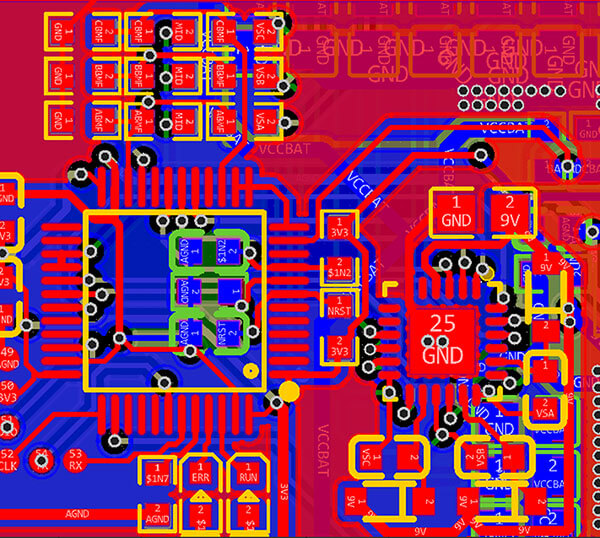
PCB Layout Definition
PCB layout involves the strategic placement of components on the board, taking into account various factors such as signal integrity, EMC, thermal design, DFM, DFT, structural considerations, safety standards, and other requirements. PCB layout is the first critical step in the entire PCB design process.
The more complex the PCB, the more the layout directly influences the ease of routing later on. The PCB layout should aim to meet the following requirements: minimize the total connection length, with critical signal paths being as short as possible; separate high-voltage, high-current signals from low-voltage, low-current signals; isolate analog signals from digital signals; separate high-frequency signals from low-frequency signals; and ensure sufficient spacing between high-frequency components. Local adjustments should be made while meeting simulation and timing analysis requirements.
FAQs
The basic design process includes six steps.
1.Concept. After identifying the need for a PCB, the next step is determining the board's final concept.
2.Schematic. The next phase is to draw the circuit schematic based on the final concept.
3.Board-Level Block Diagram.
4.Component Placement.
5.First-Pass Routing.
6.Testing.
*Source:https://www.mclpcb.com
A PCB layout is like a 3D model of a circuit board, which contains accurate information about the component placement, their sizes, pads, signal tracks width, hole diameter, etc. A PCB schematic is a blueprint for the layout. It is essential for reverse engineering the printed circuit board.
*Source:https://www.nextpcb.com
- Understand the electrical parameters.
- Creating the schematic.
- Use a schematic capture tool to create your PCB layout.
- Design your PCB stackup.
- Define design rules and requirements.
- Place your components.
- Insert drill holes.
- Route the traces.
*Source:https://www.cirexx.com
IPC-2581: A generic standard used when sending information between a PCB designer and a manufacturer or assembly company. It provides a standardized format for exchanging design data that helps ensure consistent production results. IPC-2221: The standard guideline for the process of designing PCBs.
*Source:https://www.mclpcb.com
Zero Defect
Quick-turn service
PCBA Manufacture
Learn how Keep Best can turn your designs into products.