Buried Vias Definition
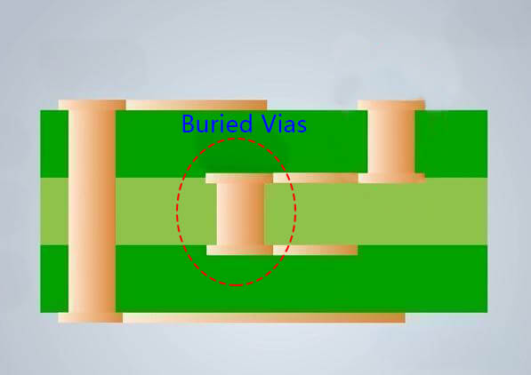
Buried vias are connection holes located within the inner layers of the PCB that do not reach the surface of the circuit board. Since both the top and bottom of buried vias are confined to the inner layers, they are not visible from the surface and do not take up any surface area, which increases the available space for surface routing. However, the manufacturing cost of buried vias is quite high, so they are not commonly used in standard electronic products. They are typically found in high-end products and are generally used in PCBs with six or more layers.
FAQs
Also buried vias require more time in manufacturing and are more expensive than regular PCBs. Buried vias are not produced at every manufacturing place as this process requires modern technology and too much attention in manufacturing.
*Source:https://www.viasion.com
Blind and Buried Vias Design
Blind and Buried via holes for each connection level must be defined as separate drill files. The ratio of blind via's drill diameter to hole depth (aspect ratio) must be 1:1 or larger, and that of buried vias must be 1:12 or larger. Blind vias can be placed within pads (via in pad).
*Source:https://madpcb.com
In a printed circuit board (PCB), a buried via connects two or more inner layers without reaching the outer layer. In comparison, a blind via connects the exterior layer about one or many middle layers. Micro vias are a more compact alternative to blind and buried vias and connect neighboring ring layers.
*Source:https://www.autodesk.com
Zero Defect
Quick-turn service
PCBA Manufacture
Learn how Keep Best can turn your designs into products.

