


Ever wondered what is SPI in SMT? And if you have had trouble with soldering parts in electronics perfectly, SPI could be the answer. But in Surface Mount Technology, it is very important to get the solder paste done properly to ensure reliable products. SPI checks out defects early on before parts are soldered.
So in this article, we will discuss what SPI is, how it works, its uses, and how it compares with other inspections like AOI. Knowledge of SPI leads to the improvement of quality control and streamlining manufacturing.
So, let’s get started.
What is SPI in the SMT Process
Accurate application of solder paste is critical in the manufacturing of electronic products to make it reliable and work right. SPI in SMT is a control point of the utmost importance throughout the production process, which carefully checks the quality of printed solder paste on PCBs prior to component mounting and soldering.
How does SPI work
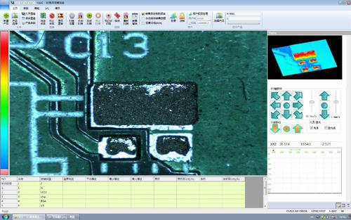
The SPI systems incorporate the latest facilities for light and camera technologies. These technologies are used for evaluating the performance of solder paste deposited on a PCB. The techniques detect all imperfections, including insufficient or excess solder, stencil bridging, solder balling, and voids.
This early detection capability allows manufacturing houses to rectify the fault before further assembly, hence saving valuable time and the cost of materials.
Benefits of SPI
Here are some important benefits of SPI:
1.Early Defect Detection and Correction
SPI inspects the solder paste for defects extremely early in the manufacturing process, before parts have even been placed on the board.
Early detection helps manufacturers correct problems more speedily, minimizing the potential for expensive rework and enhancing the reliability of products coming into the market.
2.Improved First-Pass Yield
By catching defects early, SPI contributes to a higher first-pass yield in PCB assembly.
This translates into fewer defective parts, which correspondingly reduces scrap and increases throughput to save time and costs for rework.
3.Enhancing Quality Control
SPI plays a crucial role as a conveyor of consistent quality standards down the line of electronic manufacturing.
It makes sure that solder paste deposition meets specifications, averting defects such as insufficient or excessive solder, stencil bridging, solder balling, and voids.
SPI would ensure constant quality control, leading to customer satisfaction in terms of the delivery of very reliable and defect-free electronic products.
Types of Solder Paste Defects Identified by SPI
SPI can detect a number of solder paste defects, including:
- Stencil Bridging: Solder paste bridging occurs between adjacent pads.
- Solder Balling:Forms small solder balls due to excessive paste application.
- Insufficient or Excessive Deposits:Leads to poor solder joints.
- Voids:Air pockets within solder paste affecting conductivity and strength.
Optimizing SPI Settings
Some of the factors that have to be considered for SPI optimization to ensure the inspection of solder paste on PCBs is effective include:
Factors Affecting SPI Optimization
SPI performance depends on:
- Lighting Conditions:Adequate lighting should be provided to clearly visualize the solder paste details on the PCBs.
- Camera Resolution:Higher resolution cameras capture finer details, crucial for detecting small defects.
- Inspection Parameters: Parameters such as threshold levels and defect criteria are set to fine-tune the accuracy of defect detection.
Importance of Optimization
It is necessary to optimize the SPI settings for:
- Different Solder Paste Types:Each type requires specific settings to accurately detect its unique characteristics.
- PCB Designs:Varied designs affect how solder paste is applied, demanding customized inspection settings.
By adjusting these settings, manufacturers increase the effectiveness of SPI for identifying defects at an early stage of producing electronic high-quality PCB assemblies.
Interpreting SPI Data
After inspecting solder paste on PCBs, SPI generates data that needs interpretation to ensure quality control:
- Analyzing Defects:SPI identifies issues like insufficient solder, excess solder, stencil bridging, solder balling, and voids. Analyzing these defects helps pinpoint manufacturing problems.
- Data Visualization:SPI provides visual representations of solder paste quality across PCBs. Manufacturers analyze these images to understand distribution and consistency.
- Root Cause Identification:By interpreting SPI data, manufacturers can trace defects back to specific process steps or equipment settings. This facilitates corrective actions to improve production quality.
- Continuous Improvement:Regular analysis of SPI data supports ongoing process optimization and quality enhancement efforts.
SPI vs. AOI (Automated Optical Inspection)
SPI and AOI or Automated Optical Inspection are both critical processes in SMT assembly, but they serve different purposes:
SPI (Solder Paste Inspection):
- Purpose: SPI checks if solder paste is applied correctly on PCBs before parts are added.
- Process: It uses cameras to scan the PCB and compare it to the design to find issues like too much or too little solder paste.
- Benefits: Helps prevent problems like bad connections or weak joints by catching mistakes early.
AOI (Automated Optical Inspection):
- Purpose: AOI checks PCBs after parts are soldered to find mistakes like missing parts or bad soldering.
- Process: It uses cameras to look for errors in component placement, solder joints, or PCB damage.
- Benefits: Makes sure PCBs are built correctly, reduces mistakes, and improves the quality of the final product.
Advanced SPI Techniques
Advanced SPI includes techniques like 3D inspection and integration with process control systems:
- 3D Inspection:Measures solder paste height and volume, enhancing accuracy.
- Integration with Process Control: Real-time monitoring and adjustment improve quality assurance.
Troubleshooting SPI Detection Errors
SPI may encounter issues like false positives/negatives:
- False Positives:Incorrectly identifies defects that aren’t actually present.
- False Negatives:Fails to detect actual defects.
Regular calibration and maintenance are essential for reliable SPI performance:
- Calibration:Ensures accuracy in detecting solder paste defects.
Maintenance: Keeps equipment functioning optimally, reducing detection errors.
Conclusion
In conclusion, SPI is crucial in SMT for ensuring accurate solder paste application before component soldering. By leveraging advanced light and camera technology, SPI detects and rectifies defects like insufficient solder, excess paste, stencil bridging, solder balling, and voids early in the manufacturing process.