


Are you having trouble with BGA soldering on your PCBs? Today, there are several companies working with components like Ball Grid Arrays, and understanding it can be a headache due to the design intricacies and high-density connection.
But fear not as this article is going to walk you through all the complexities. Whether you are just embarking upon electronic assembly or looking for perfect fine-tuning, it becomes imperative to understand the nuances of BGA technology.
From the basic knowledge of BGA structure up to step-by-step soldering direction and troubleshooting tips, this guide is going to help you. In the end, you will be certain regarding the whole BGA process to ensure reliable connections and perfect performance in your electronic devices.
So let’s begin.
What is a Ball Grid Array (BGA)
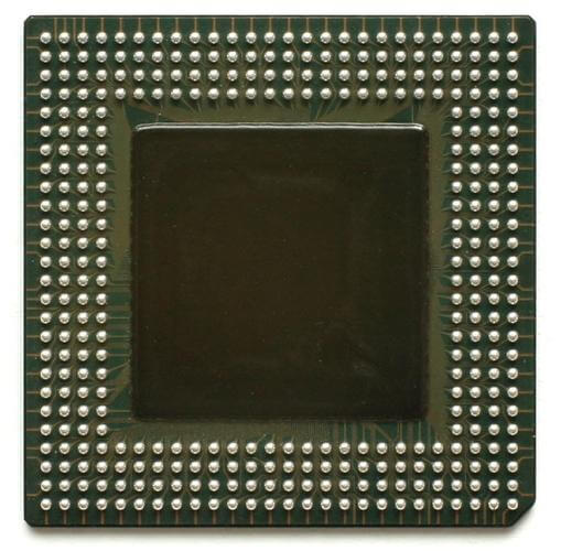
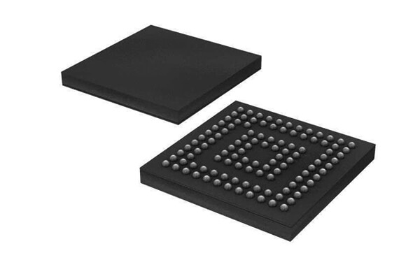
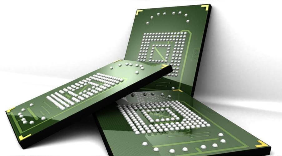
A Ball Grid Array, or BGA, is a newer type of surface-mount packaging installed onto integrated circuits inside electronic gadgets. BGAs differ from the older positioned grid arrays mainly in terms of their solder balls located on the lower side of the integrated circuit package, which connect directly to the PCB.
Furthermore, this defines a kind of packaging design with high-density connections, and thus in a much smaller area, more connections can be accommodated compared to packages like QFPs.
BGAs are preferred in modern electronics for several reasons. Its small size helps manufacturers design smaller and lighter devices, which is very appropriate for such portable electronics as smartphones and tablets.
Moreover, the direct attachment of the solder balls to the PCB optimizes electric performance and brings about reliability through a reduction in lead inductance and improvements in the integrity of the signal.
Structure of a BGA Package
A usual Ball Grid Array package has the following few functional and reliable components that enable it in electronic gadgets:
- Substrate:A mounting base material for the BGA package, usually a non-conductive material such as fiberglass (FR4), to provide mechanical support and electrical insulation.
- Solder Balls:These are small spheres of solder located literally at the bottom of the BGA. They are how the IC inside the package makes electrical and mechanical connection to the PCB. After careful alignment of the solder balls, it is placed in the matching position with the corresponding pads on incoming PCB for proper electrical contact.
- Die Attach Pad:It is the area within the pattern of BGA in which an IC chip is put or affixed. In general, the IC chip is attached to the die-attach pad using conductive epoxy or solder paste.
- Wire Bonds:Wire bonds connect the bond pads on the IC chip to the internal circuitry of the BGA package Substrate. It provides for electrical connectivity between the IC and the package substrate.
- Encapsulation:The entire structure is encapsulated with a protective material (epoxy resin or molding compound) to shield the sensitive IC chip, wire bonds, and internal connections from mechanical damage, moisture, and other environmental factors.
This knowledge of the composition and structure of a BGA package forms the core of designing and assembling PCBs effectively to enable the reliable operation of electronic gadgets.
Now let’s discuss the different types of BGA packages you should get to know.
Types of BGA Packages
BGAs come in various types, which find application based on differing requirements of size, heat dissipation, and electrical performance in electronic devices.
Knowing the different types will let you decide on the BGA package that best suits your application:
- Standard BGA (sBGA):This is the most common type of BGA package, characterized by a regular array of solder balls underneath the package. Standard BGAs offer good thermal and electrical performance and are widely used in consumer electronics.
- Thin BGA (TBGA):The TBGA is much like the standard BGA, but it is thinner in profile, hence suitable to be used, for example, in all sorts of devices with relatively rigid height conditions, from mobilе products to thin-notebook computеrs.
- CSP-BGA (Chip-Scale Package BGA):CSP-BGA stands for chip-scale package ball grid array. CSP-BGA packages are designed to have a footprint almost as small as the Integrated Circuit (IC) chip that they contain, allowing minimum PCB area coverage. Most widely used in applications requiring high-intensity relevant to great thermal management.
Each type of BGA package has its advantages and is chosen based on factors like board space, thermal management requirements, and cost considerations.
It allows a designer to optimize the performance and reliability of an electronic product by choosing the right kind of BGA.
Advantages and Disadvantages of BGA
BGA packages offer several advantages and disadvantages compared to traditional packaging methods like Quad Flat Packages (QFPs).
Understanding these can help in making informed decisions during PCB design and assembly:
Advantages:
- Higher Density Connections:BGAs provide a higher number of connections (pins) in a smaller footprint compared to QFPs. This makes them ideal for compact electronic devices where board space is limited.
- Improved Electrical Performance:The direct connection of solder balls to the PCB results in lower lead inductance and improved signal integrity. This enhances the electrical performance of BGAs, making them suitable for high-frequency applications.
- Better Thermal Management:BGAs typically feature a large thermal pad underneath the package, which enhances heat dissipation. This is crucial for components that generate significant heat during operation.
- Reduced Risk of Damage:The solder balls on BGAs are less susceptible to mechanical stress and vibration compared to leads on QFPs, reducing the risk of solder joint failure.
Disadvantages:
- Complex Rework:Due to their compact design and the need for precise soldering techniques, reworking BGAs can be challenging and may require specialized equipment and skills.
- Higher Cost:BGAs may be more expensive to manufacture and assemble compared to QFPs, primarily due to the precision required in the soldering process and the materials used.
- Testing Limitations:Testing BGAs for defects or faults can be more challenging compared to QFPs, as access to the solder balls for testing purposes is limited.
- Potential for Solder Joint Issues:Improper soldering techniques or environmental factors can lead to issues such as solder bridges or cold joints, affecting the reliability of the BGA connection.
Despite these challenges, the advantages of BGAs often outweigh the disadvantages, especially in applications where size, performance, and reliability are critical factors.
BGA Assembly Process
The assembly of Ball Grid Array packages on printed circuit boards requires careful planning and precise techniques to ensure reliable connections and optimal performance.
Here’s an overview of the BGA assembly process:
1. Design Considerations
Designing the PCB layout to accommodate the specific dimensions and pitch of the BGA package is crucial. Properly designed footprints ensure accurate alignment of solder balls with PCB pads.
Selecting the right type of solder paste and flux is essential for achieving good solder joints. Lead-free solder alloys are commonly used due to regulatory requirements and environmental concerns.
2. Stencil Printing for Solder Paste Application
A stainless steel stencil is used to precisely deposit solder paste onto the PCB pads where the BGA will be mounted. This step is critical for achieving uniform and controlled solder deposition.
3. Reflow Soldering Techniques for BGAs
During reflow soldering, the entire PCB assembly, including the BGA, is heated in a controlled environment to melt the solder paste. The surface tension of the molten solder balls ensures proper wetting and formation of reliable solder joints.
Proper temperature profiles and heating rates are crucial to prevent issues such as solder ball collapse or insufficient solder joint formation.
4. Quality Control and Inspection Processes
- X-ray Inspection:Due to the BGA’s hidden solder joints, X-ray inspection is often used to verify solder joint integrity and detect defects such as voids or misalignments.
- Visual Inspection:Post-reflow visual inspection is conducted to check for solder bridges, opens, or other visible defects.
- Electrical Testing:Functional testing of the PCB assembly, including BGA components, ensures that all connections are electrically sound and meet performance specifications.
By following these steps diligently, manufacturers can achieve high yields and reliable BGA assemblies for their electronic products.
Practical Tips for Working with BGAs
Working with BGAs requires attention to detail and specific techniques to ensure successful assembly and troubleshooting.
Here are some practical tips to guide you:
1. Use the Right Tools and Materials
To solder BGAs effectively, use tools like a fine-tipped soldering iron or a hot air rework station. These tools provide precise control over heat, crucial for soldering small components like BGA solder balls.
Keep solder wick handy to remove extra solder and apply flux to ensure good solder joints.
2. Understand the Soldering Process
Prepare by preheating the PCB to prevent thermal shock. Use a stainless steel stencil to apply solder paste evenly on PCB pads.
Follow the solder paste manufacturer’s reflow profiles for even melting of solder balls. Inspect visually during and after soldering to catch issues like solder bridges.
3. Follow Proper Soldering Techniques
During reflow soldering, follow temperature profiles carefully to melt solder balls uniformly. Inspect visually to ensure solder balls are aligned and melted correctly. After soldering, check for issues like solder bridges and fix with flux and a soldering iron.
4. Handle with Care
Handle PCBs with BGAs carefully to avoid damaging solder joints. Avoid mechanical stress during assembly and control humidity and temperature to prevent moisture absorption and thermal shock.
5. Troubleshoot Common Issues
To fix solder bridges, use solder wick or a fine-tipped soldering iron for precise solder removal. Address open or cold joints with additional flux and controlled reflow to ensure reliable electrical connections.
Final Words
Understanding everything about Ball Grid Array soldering is crucial for building reliable electronic devices.
By using the right tools, understanding the soldering process, and handling BGAs with care, you can ensure strong electrical connections and avoid common issues like solder bridges.
Remember to follow proper soldering techniques and conduct thorough inspections to guarantee quality. With these practices, you will be well-equipped to tackle BGA assembly confidently, leading to efficient and dependable electronics for various applications.