


Wondering what is GND in a PCB? Fighting with the grounding issues of your designed Printed Circuit Board? You are not alone. Many designers experience problems with signal integrity, noise, and electromagnetic interference due to improper grounding.
But do not worry as this guide is here to help you. We will break down everything you need to know about GND in a PCB—from very simple to the most advanced techniques.
Let’s get started.
What is GND in PCB
Ground, in the electronics domain, is usually a reference point within an electrical circuit from which voltages are measured. Electric current finds its way back to the ground through it, ensuring that a circuit works right and does not burn out due to an overflow of electric potential difference.
In other words, a ground is just like a baseline or a zero-voltage point against which all other voltages in a circuit refer. Proper grounding is very fundamental for the stable operation of an electronic circuit while it helps to retain signal integrity and reduce noise.
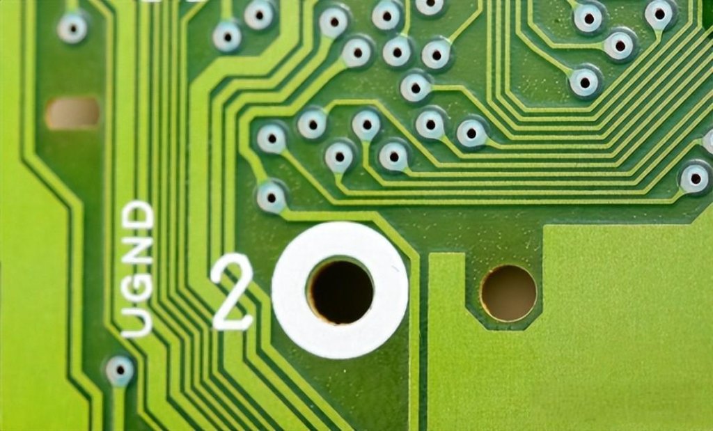
Ground is essential in printed circuit boards. GND in PCB simply means areas or planes that are dedicated to providing a reference point for the measurement of all voltages on the board.
These ground planes or areas provide a stable reference voltage to the components so that the circuit performs its job. A good grounding in a PCB reduces noise, minimizes the generation of EMI, and helps retain the integrity of the signals across the board.
Importance of Grounding in PCBs
The significance of grounding in the printed circuit board is very important for:
- Signal Integrity
Proper grounding provides utterly clean and consistent flow to the signal levels in a circuit. This will give a very stable reference, typical in a circuit, essential in maintaining the integrity of the signals—very critical, especially in high-speed digital circuits.
- Noise Reduction
Grounding helps keep unwanted electrical noise from getting in the way of signal transmission and the general operation of a circuit. Proper grounding provides a definite path for noise dissipating, ensuring its reliability in a PCB.
- Electromagnetic Interference (EMI) Reduction
Adequate grounding ensures minimal electromagnetic interference emitters and susceptibility resulting from high-frequency currents. This is particularly so in environments with many electronic devices running simultaneously.
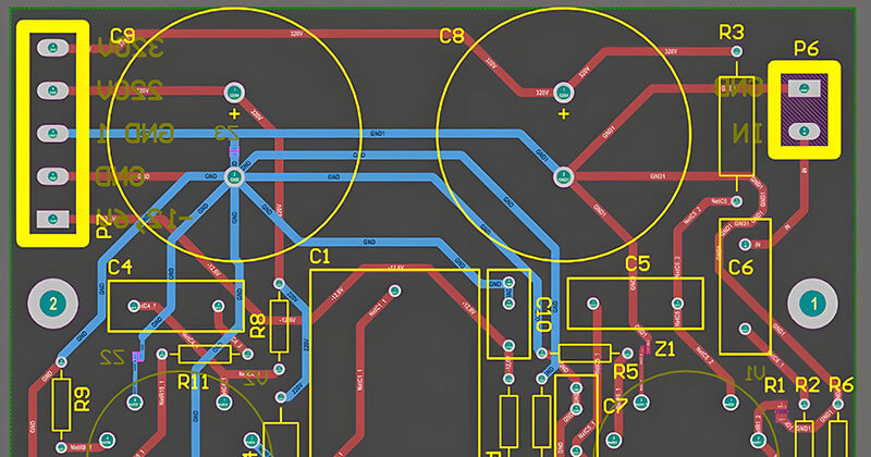
Understanding Ground Planes
Ground planes are areas of dedicated copper on a PCB, and they provide, for the most part, a reference for ground in the circuit.
These planes play a significant role in ensuring a stable ground potential over the whole board to protect signal integrity and minimize noise.
- Function as the GND Reference: Ground planes provide all components on a PCB with a common reference point. This ensures that a consistent voltage reference to all the signals is provided, often being the key for a circuit to run correctly.
- Improved Grounding Performance in Multi-Layer PCBs: A multi-layer printed circuit board may have multiple ground planes. Designers can segregate different ground planes into varying layers for more effective grounding. More effective grounding will reduce EMI and improve the overall reliability of the PCB.
Benefits of Using Ground Planes
- Signal Integrity: It is because of the low-impedance path that ground planes provide for return currents, thus helping to maintain the integrity of high-speed signals.
- Noise Reduction: The ground planes, offering a large area for the dissipation of unwanted noise, help in reducing electrical noise that can affect the performance of the circuit.
- EMI reduction: Effectively, island-style ground planes reduce emissions and susceptibility to electromagnetic interference in this way, making a PCB more rugged against noisy environments.
Knowing the nature and implementation of these ground planes in your PCB design will ensure stable and reliable operation for circuits, simple or complex, in any electronic system.
Types of Grounding Techniques
Effective grounding is essential for maintaining the performance and reliability of PCB designs. Here, we’ll explore three common grounding techniques used in PCB design: Single-Point Grounding, Multi-Point Grounding, and Star Grounding.
Each method has its advantages and limitations, making them suitable for different types of circuits.
Single-Point Grounding
Single-point grounding involves connecting all ground points in a circuit to a single location. This method creates a single reference point for the entire system.
Advantages:
- Simplicity: Easy to implement in simple circuits with few components.
- Reduced Ground Loops: Minimizes the risk of ground loops, which can cause unwanted noise and signal interference.
Limitations:
- Unsuitable for Complex Circuits: In complex circuits with multiple high-speed signals, single-point grounding can lead to long ground paths, increasing the risk of noise and signal integrity issues.
- Limited Current Handling: May not be able to handle large return currents efficiently.
Multi-Point Grounding
Multi-point grounding involves connecting ground points to multiple locations across the PCB. This method is often used in more complex circuits to provide better grounding performance.
Advantages:
- Improved Grounding for Complex Circuits: Provides multiple paths for return currents, reducing the risk of ground loops and noise.
- Enhanced Signal Integrity: Shorter ground paths help maintain signal integrity, especially in high-speed designs.
Limitations:
- Complex Implementation: Requires careful planning and design to avoid creating ground loops.
Potential for Increased Noise: If not designed properly, multiple ground connections can introduce noise into the system.
Star Grounding
Star grounding involves connecting all ground points to a central star point. This technique is effective for high-frequency circuits where signal integrity is crucial.
Advantages:
- Minimized Ground Loops: Central star point reduces the risk of ground loops, ensuring clean signal paths.
- Effective for High-Frequency Circuits: Provides clear and direct grounding paths, essential for maintaining signal integrity in high-frequency designs.
Limitations:
- Complex Routing: Requires careful routing to ensure all ground points are connected to the central star point without introducing unwanted noise.
- Limited Suitability for Large Systems: In very large systems, the central star point can become overloaded, reducing its effectiveness.
Considerations for Effective Ground Plane Design
Designing an effective ground plane is crucial for the performance and reliability of PCBs. Here are some practical tips to help you optimize your ground plane design:
Copper Distribution
Maximize the copper coverage to create a low-impedance path for return currents. Allocating as much continuous copper area as possible for the ground plane helps maintain signal integrity and reduce noise.
Avoid breaks and gaps in the ground plane, as they can create high-impedance paths leading to signal issues. In single-sided PCBs, use any unused areas for the ground plane. For multi-layer boards, dedicate at least one entire layer to the ground plane to ensure a stable and effective grounding system.
Via Placement
Use vias to connect ground planes on different layers of a multi-layer PCB. This helps maintain a continuous grounding path across all layers, enhancing the overall grounding performance. Place vias strategically to minimize the length of signal return paths.
Shorter paths mean return currents can travel more directly to the ground, reducing noise. Position vias close to the ground pins of components to ensure efficient current return paths, minimizing noise and electromagnetic interference (EMI).
Grounding Rules
Maintain adequate separation between signal traces and the ground plane to reduce the risk of crosstalk and signal interference. Establish minimum clearance rules for traces running close to the ground plane to help in noise reduction and prevent unwanted coupling.
Ensure that high-current paths do not cross sensitive signal traces, as high currents can induce noise and affect signal integrity. Implement guard traces connected to the ground plane around sensitive signal traces. These guard traces act as a barrier to electromagnetic interference, further enhancing the performance and reliability of the PCB.
Troubleshooting Grounding Issues
Troubleshooting grounding issues is crucial for maintaining signal integrity and minimizing noise in electronic circuits. Here are some guidance points for identifying and resolving common grounding problems:
Identify Noise Sources
- External Sources:Electromagnetic interference (EMI) from nearby devices, power lines, or radio frequencies.
- Internal Sources:Switching power supplies, high-current circuits, or improperly shielded components.
Mitigation Strategies
- Proper Grounding Techniques:Ensure all components share a common ground point to prevent ground loops.
- Ground Plane Design:Optimize PCB layout to minimize noise coupling by using dedicated ground planes or traces.
- Filtering:Implement low-pass filters or ferrite beads to attenuate high-frequency noise.
Effects of Grounding Problems
- Ground Loops:Cause unintended current paths leading to noise and signal distortion.
- Voltage Drops:Uneven ground potentials can affect voltage references and signal levels.
Diagnosis and Resolution
- Check Ground Connections:Ensure all ground connections are secure and low-impedance.
- Inspect PCB Layout:Verify that sensitive analog and digital circuits are properly separated and grounded.
- Use Differential Signaling:Differential pairs can mitigate common-mode noise by canceling out interference.
By addressing these aspects methodically, you can effectively diagnose and resolve grounding issues that may impact both noise levels and signal integrity in electronic circuits.
Final Words
In conclusion, mastering effective grounding techniques in PCB design is essential for achieving reliable performance. A well-planned ground plane, careful via placement, and following grounding rules are key to reducing noise, preserving signal quality, and minimizing electromagnetic interference.
By addressing typical grounding challenges like noise and signal issues with clear identification and solutions, engineers can ensure their PCBs operate smoothly and consistently.