


Edge plating is an exact and essential, yet mostly ignored feature of PCB production. Does your PCB have an exposed edge that’s likely to corrode and get damaged?
It is a common issue, and it compromises your circuit boards’ performance and durability. However, the good news is that there is a solution for both.
In this article, we explain everything about edge plating: What it is, why it’s essential, and how it can significantly improve the reliability of your PCBs.
After reading this article, you will be in an excellent position to protect your PCBs adequately and guarantee they work to their highest capacity in each environment.
So, let’s do this.
What is Edge Plating
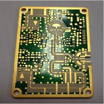
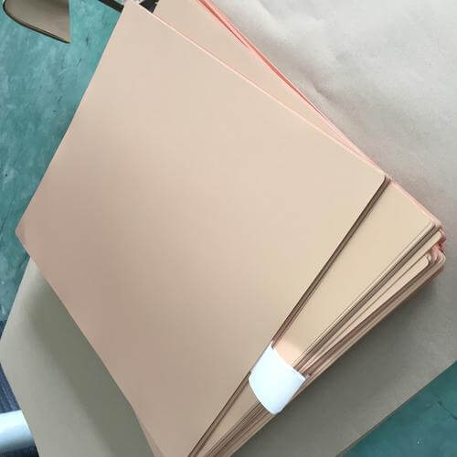
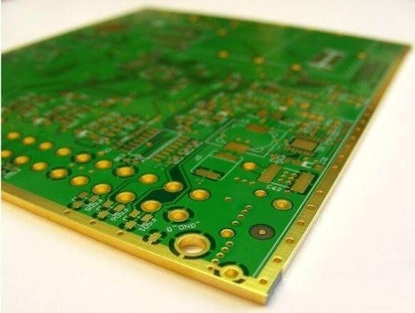
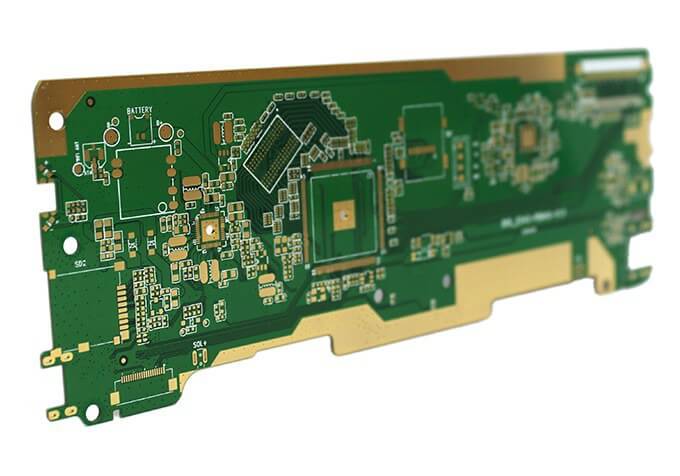
Edge plating involves plating a thin layer of metal on the exposed edges of a PCB to assure improved functionality and life span. This thin sake of metal layer, like nickel or gold, deposited shall be of protection against corrosive attacks at the edges. It also provides a much smoother surface to solder components onto.
Besides, the edge plating can also make a board look more complete. But this would not be the only function that the edge plating has. Through these elementary facts of the environmental shield for copper layers of the PCB, it dramatically increases the performance, as well as longevity.
2 Main Reasons for Edge Plating
Edge plating is majorly used in PCB manufacturing for two primary purposes:
- Improved Solderability
One of the significant advantages of edge plating is a smooth, flat surface that makes it much easier and offers more assurance on the reliability of solders for parts on the edge.
This will help to ensure solid and durable joints, which are two essential aspects of keeping the integrity of electrical connections. The well-plated edge will always ensure that there is a lesser possibility for defects like poor adhesion and weak joints during soldering.
- Enhanced Corrosion Protection
The exposed copper edges are especially subject to various environmental risks, such as different kinds of abrasive liquids, depending on the level of impurities, and may lead to corrosion after some time.
The copper is shielded from such elements by the edge plating, which is hard, thus enabling the preservation of electrical performance.
This ensures continued conduction and, thus, functionality of the device electronics by avoiding any possible corrosion due to exposed edges.
Types of Edge Plating
There are two main types of edge plating commonly used in PCB manufacturing:
1.Electroless Nickel/Immersion Gold (ENIG)
ENIG is the most common type of edge plating, known for its excellent solderability and corrosion resistance. In this process, a layer of nickel is deposited followed by a layer of gold on the exposed edges.
Nickel furnishes a hard, durable base, while gold furnishes superior solderability and oxidation protection. ENIG is applicable for applications with high reliability and performance.
2.Hot Air Solder Leveling (HASL)
It is a relatively inexpensive finish for plating PCBs edges. In HASL, solder is applied to the edges of the PCB and leveled with hot air. HASL is generally cheaper than ENIG, but it has the disadvantage of less solderability and corrosion resistance.
Nevertheless, it remains a very viable option for many applications, particularly those where cost is a crucial factor.
Edge Plating Process
A bunch of steps accompanies the edge plating process to ensure that the exposed edges of the PCB are protected and adequately treated to ensure the most reliable performance.
The general overview of the process includes:
1.Surface Preparation
The initial step is preparing the surface by cleaning and roughening the edges of the metal, to allow for adhesion when the metal layer applied passes through plating and bonds with the metal of the copper.
This is carried out for the cleaning process to remove all forms of contaminants, which in most cases manufacture oxidation and residues that may later act to retard the plating process. The roughing of the edges tends to give it a texture that permits good mechanical bonding during the copper plating.
2.Plating
Following preparation, the next process is plating. The edge that has undergone preparation upon performing different techniques needs to have a desired metal layer deposited over it.
The two main techniques are:
- Electroless Nickel/Immersion Gold (ENIG):This method involves an electroless plating process to apply a layer of nickel followed by a layer of gold. The nickel acts as conditioning underneath the hard gold applied, and the gold atop acts as protection of nickel from oxidation. Generally, solderability is good, and electrical conductivity demonstrates excellent values.
- Hot Air Solder Leveling (HASL):In this cost-effective method, solder is applied to the edges of the PCB and leveled using hot air. While it doesn’t have the excellent solderability and resistance to corrosion that ENIG does, this is a suitable substitute for many applications when the cost is essential.
3.Final Finishing
The optional finishing is when a second protection is given in the last stage of the edge plating; this treatment is not always necessary but offers even more durability and look to the PCB.
Depending on the application requirements, a protective coating or additional metal layer may be applied to ensure long-lasting performance and reliability.
Benefits and Applications of Edge Plating
Edge plating is highly advantageous in PCB manufacturing, providing several huge benefits like:
Key Advantages
- Increased Solder Joint Reliability and Strength
Edge plating ensures smooth, uniform surfaces, making the components align themselves more securely with the circuit board – as well, that soldering features greater ease and increased reliability.
This automatically equates to highly reliable soldered joints, giving utmost certainty to the integrity of the electrical connections regarding a low probability of a flaw in the solder or breakdown of this joint over time.
- Improved Resistance to Corrosion and Environmental Factors
Edge plating is a barrier to all environmental elements, such as moisture, humidity, and chemicals, that would cause corrosion. This offers protection to the exposed copper edges, hence maintaining and preserving the electrical performance of the PCB while extending its life even under adverse conditions.
- Enhanced Aesthetics and Professional Appearance of the PCB
It helps the printed circuit board to take on a clean look and appear very professional overall. It can be essential in consumer electronics and other applications where a high aesthetic quality competes with the overall build quality.
Common Applications
Edge plating is especially beneficial in the following applications:
- High-Reliability Electronic Devices
Devices such as medical equipment and aerospace systems require the utmost reliability and durability. The assurance given with edge plating plays an essential role in ensuring such critical devices maintain strong, reliable, and corrosion-resistant connections.
- Consumer Electronics with Exposed Edges
Devices like smartphones, laptops, and tablets often have exposed edges that can be subject to wear and damage. This form of edge plating would hence come in handy to protect such edges from corrosive actions, enhancing the beauty of such devices and adding to their quality of life.
- PCBs Operating in Harsh Environments
PCBs with high humidity, extreme temperature, or chemical exposure conditions witnessed in the area could gain a lot from edge plating. The protective metal applied will thus protect the printed board from harsh conditions and ensure that it maintains high performance without the most chances of failure.
By incorporating edge plating into the PCB manufacturing process, manufacturers can significantly enhance the reliability, durability, and appearance of their circuit boards, making them suitable for a wide range of demanding applications.
Design Considerations for Edge Plating
For successful edge plating, several design factors must be considered to ensure optimal performance and reliability of the PCB.
- Minimum Clearance Between Circuit Features and the Board Edge
Some clearance should exist between the circuit features and the board edge, generally 0.025 inches, to ensure no short circuit or interference can emerge during the plating process or at a later stage of operations.
This helps to ensure that the plating material is evenly deposited onto the plated edges, offering constant protection throughout and in performance.
- Size and Shape of the Exposed Edges
The size and shape of the exposed edges would be made to facilitate effective plating. Uneven edges reduce the adhesion of the material for plating and increase the possibility of defects.
It is expected to prefer rounded or beveled edges as the opposite, sharp corners or irregular shapes could result in a lack of even plating and the possible creation of weak points.
- Compatibility of the Plating Material with the Intended Soldering Process
Soldering needs good adhesion between the plating and the substrate material. Thus, the proper choice of the plating material with the solder process is critical. Strong adhesion, representing the ease of a good solder joint, remains a must-to criterion to generate a practical, sound joint.
For instance, ENIG (Electroless Nickel/Immersion Gold) is one of the most desirable, containing features such as excellent solderability and outstanding corrosion resistance, and works well for high-reliability applications.
In contrast, HASL (Hot Air Solder Leveling) is an inexpensive option, but it may offer lower solderability and corrosion resistance, which grants it applicability to needs of lesser demand.
Thus, in taking these factors under consideration in the design aspect, the manufacturers may guarantee the process of edge plating with the desired effectiveness to come out with well-built and trustworthy PCBs that meet the minute demands of the applications into which they are fed.
Final Words
In conclusion, edge plating is a vital process in PCB manufacturing that enhances the durability, functionality, and appearance of circuit boards.
This helps shield the PCBs for optimal performance in various environments.
Whether for high-reliability devices, consumer electronics, or PCBs used in harsh conditions, edge plating provides the necessary protection and reliability to maintain strong, durable connections.