


PCB panelization is an efficient way to optimize the making of multiple printed circuit boards. Are you wrangling with the complexity of producing a high volume of PCBs in addition to attempting to cut costs and better quality?
You are not alone. Most manufacturers face similar problems. But don’t worry at all as this article will walk you through the PCB panelization’s ins and outs, offering practical insights into using various techniques with the best practices.
In the end, you will know how to reduce your manufacturing process, save money, and make your PCBs better.
So, let’s get started.
What is PCB Penalization Manufacturing
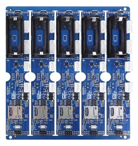
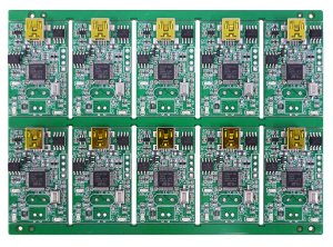
PCB panelization manufacturing is a process by which several Printed Circuit Boards are produced from a single, large panel. This is a process by design of one giant board consisting of several small PCBs, which are to be divided after being manufactured.
This is required for optimal production efficiency and lower costs in high-volume manufacturing environments for the best possible quality.
Key Advantages of PCB Panelization for High-Volume Production
Critical benefits of PCB penalization for high-volume production include:
- Increased Efficiency
One of the significant benefits of PCB panelization includes the ability to fabricate and assemble several PCBs simultaneously. The fact that these manufacturers work on larger panels that have more than one PCB aims at reducing the total time that increases in the production chain to come fast.
The process is made time-friendly in that different boards go through each stage in the production process concurrently, which ranges from fabrication to assembly, thereby speeding the whole cycle for several boards.
- Reduced Costs
Apart from saving materials, PCB panelization also helps seal off wastages while utilizing opportunities for as much as possible of the needed manufacturing processes.
In other words, packing as many PCBs as possible into one panel dramatically reduces the number of remnants that are laid to be in the waste, as the duplexing process ensures that no PCB is wasted during their production.
What conserves the utilized resource is the corresponding lower expenses incurred within manufacturing products en masse.
- Improved Handling
Larger panels are easier to handle and transport than single PCBs. The logistics of handling one large panel compared to many small boards are simplified, and an order of magnitude improvement in transport safety can be achieved.
Such enhanced handling efficiency is even more beneficial on an automatic assembly line, wherein precision, and by extension speed, is the watchword.
- Enhanced Quality Control
Panelizing PCBs improves group testing and inspection, apparently improving the general quality of consistency. Through collective examination and testing of several issues at a go, defects are easily located at early stages.
More time is also saved during testing; therefore, standards are fully met before separation into individual units. Better quality control can make products much more more reliable and allow cost-efficient rework or recalling of products that have already been manufactured.
All these advantages can be achieved by the different techniques of PCB penalization. Let’s discuss them in detail.
PCB Panelization Techniques
The following are some common PCB panelization techniques:
1.V-cut Panelization
In V-cut panelization, the boards ready to use in PCBs are seamed together by scored lines and located in proper positions throughout the panel. The scored lines create a V-shaped groove, which can partially or entirely cut through the thickness of the panel.
These boards are easily broken from the panel after PCB fabrication and complete assembly to yield clean fracture separation of the individual boards.
2.Routing Panelization
Panelization through routing involves the axial extraction of milled grooves of routed channels in panel materials by CNC machines. The channels are usually milled around the PCB’s perimeter.
This helps separate them easily from the fabricated big panel. Boards may have to be routed when the board has complex profiles or very tight dimensions.
3.Laser Depanelization
Laser depanelization is achieved by placing the laser cutting system on the paths predefined with high accuracy along with each PCB. Very high accuracies can be maintained, and this method applied to most board designs can be of any complex nature.
The virtue is that there is no resultant mechanical or chemical stress or damage. Gen erally this method is pre ferred for applications of high pre ci sion, mechan i cal stress, or dam age is unac cept able and accu rate clean cut ting is essential.
4.Snap-Tab Panelization
In snap-tab penalization, a PCB is attached to a panel through short tabs or even bridges that let the PCB be quickly snapped or broken out from the panel.
Snap tabs mostly hold the PCB in place on the board during its production, assembly, and handling but are quickly removed in the depanelization process without tools or with minor force. Panelization with snap-tab technology is proven to be effective for mass production to facilitate faster assembly and depanelization.
All of the above panelization methods have their advantages based on the requirements of the PCB design, production volume, and precision level. The proper method will ascertain efficient manufacturing processes and high-quality products at last.
PCB Panelization Design Considerations
When designing PCB panelization, several key factors play a crucial role in optimizing manufacturing efficiency and ensuring high-quality end products:
1.Panel Size
The critical aspect lies in choosing the right panel size. Larger panels can increase the efficiency of production by running more PCBs at the same time.
At the same time, that is also the reason for the one big issue to deal with when saving material waste: the optimal panel sizing aims to make sure that little is thrown away yet efficiently handled and processed throughout the manufacturing.
2.Fiducial Marks
Fiducials provide the correct placement of components over printed wiring boards in the circuit board during assembly. In essence, they are mere landmarks, preferably minor nonfunctional marks, located strategically on the panel.
They help align and assemble components more perfectly into these automated machines during assembly thereby vouch for better overall accuracy and reliability in manufacturing.
3.Spacing and Clearance
Adequate spacing between PCBs commonly found on a panel is based on several important reasons. It allows the proper fitment of routing or V-cuts, that is, the separation of boards after fabrication.
It further saves the collision of components during the assembly processes, which not only assures the consistency of product quality but also reduces the chance of damage.
4.Tearaway Features
Tearaway features are the small copper sections attached strategically onto the board to give a clean, low-stress way to pop apart the individual PCBs after depanelization.
These features aim to minimize mechanical stress on the boards, assuring the separation of each tiny PCB without damaging the components or blowing out the circuitry.
5.Panelization Design Software
Utilizing panelization design software is crucial for efficiently creating and optimizing panel layouts. These tools automate the process of arranging PCBs on a panel while adhering to specific design rules and constraints.
This automation in creating panelization layouts would save time, reduce errors, and achieve consistency for the manufacturers.
When considered carefully in design, all these factors consequently result in the optimization of the PCB panelization process, with improvement in manufacturing efficiency and cost-effective yields of high quality.
Optimization of panels for all types of manufacturing needs rests on every consideration and assures some reliability in the design of electronic products.
PCB Depanelization Methods
Efficiently separating individual PCBs from a panel after manufacturing involves employing specific depanelization methods tailored to different production needs:
- Controlled Break
Controlled break depanelization involves applying pressure or using tools to break PCBs along pre-scored V-cut lines.
This is a straightforward and low-cost method of breaking boards with standard geometries for cutouts, with minimal risk from this process of damaging components or circuits.
- Routing Depanelization
Routing depanelization utilizes Computer Numerical Control (CNC) machines to mill precise channels around each PCB on the panel. It works out very well with complex-shaped boards or where the later dimensions are of utmost importance.
This results in immaculate edges and, thereby, very little stress on the boards as they are parted.
- Laser Depanelization
Laser depanelization involves the use of high-precision lasers to cut through a panel material, tracing predefined paths around each printed circuit board.
This method works great with very tight designs, featuring the possibility of immaculate and precise, contactless cuts while avoiding the thermal stress of components.
- Snap-Tab Depanelization
In snap-tab depanelization, PCBs are attached to panels through smaller tabs, which can afterward be easily separated by the use of hands. These are good for high-volume processing since they will enable simple separation without necessarily using any form of equipment.
That way, it minimizes handling damage throughout the process and supports high-speed assembly processes.
Each depanelization method has its advantages depending upon the design complexities of a PCB, the volume of production, and how precisely the cut quality would be.
Choosing the proper depanelization technique is very critical to maintaining the quality of products and also to optimizing manufacturing efficiency to ensure that the process is cost-effective.
PCB Panelization and Assembly Line Integration
PCB panelization plays a crucial role in optimizing Surface Mount Technology (SMT) assembly processes, enhancing efficiency, and ensuring quality throughout production:
- Pick and Place Machines
Consequently, the automated pick-and-place machines are fed information that will make them pick components from either the reels or trays precisely and place them onto designated locations on each PCB within the panel.
If there are any multiple PCBs in the panel, these same picking and placing machines will take care of them at the same time, thus aiding in obtaining the maximum throughput that minimizes the time taken during assembly.
- Soldering
All components placed in the PCBs are finally soldered by running the entire panel through a reflow oven. The temperature of the stove is precisely controlled so that the solder paste can melt, making electrical solid connections between the components and the PCB pads.
Panelization allows large volumes of PCBs to be efficiently processed with consistent results.
- Depanelization
PCBs are then separated from the panel with the help of depanelization, controlled break, routing, laser cutting, or snap-tab removal. This process is essential for handling and inspecting each final PCB to be assembled into electronic devices.
- Testing
Every devastated PCB is tested for function and performance. At this stage of SMT, an in-circuit test (ICT) can be done to capture faults and validate constituents’ property.
Panelization facilitates efficient testing by allowing multiple boards to be tested in parallel, reducing overall testing time and improving quality control.
The integration of the manufacturing processes not only reduces the production cost but also increases reliability and an end-to-end manufacturing improvement of electronic goods.
These integrated systems optimize every manufacturing process, from component placement to final testing; hence, they have overseen their PCBs, achieving resemblance to set standards before the integration into the rest of the device.
Final Words
That’s all you need to know about PCB panelization manufacturing and assembly. In terms of efficient ways of working, this increases the productivity of PCBs in areas of time, costs, and product quality through penalization techniques.
Effective penalization strategies are crucial to achieving the right balance of high volume or highly detailed PCB design.