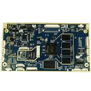
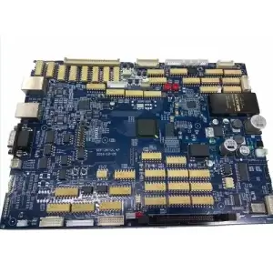
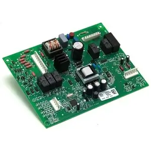
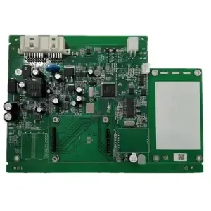
PCB Assembly
in China and Thailand
We are committed to making our Printed circuit board assembly products zero-defect and can return or exchange them for you without any reason.

Zero defects
We are committed to providing you with zero-defect products.

Trustworthy
In the pursuit of quality, we are always worthy of your trust.

Can be returned or exchanged
No physical objects, no photos, no reason to return or exchange.
Our Clients

Who We Are
We provide
the best PCB Assembly Services
One - stop Printed circuit board assembly Solution provider
Keep Best PCB Assembly Co., Ltd serves many well-known brand customers in industrial control, security, medical, Internet of Things, automotive, artificial intelligence, smart home, power and communications industries at home and abroad.
The company continues to be customer-centric, improves the level of digital intelligence, and is committed to meeting continued high-quality customer needs.
In 2024, we put forward the quality requirements of “zero defects, support for no-reason returns and exchanges” that challenge the limits of the industry, and strive to provide customers and partners with the highest quality products and services in the industry, and assist customers in business success.
What We Offer
Full Turnkey PCB Assembly Services
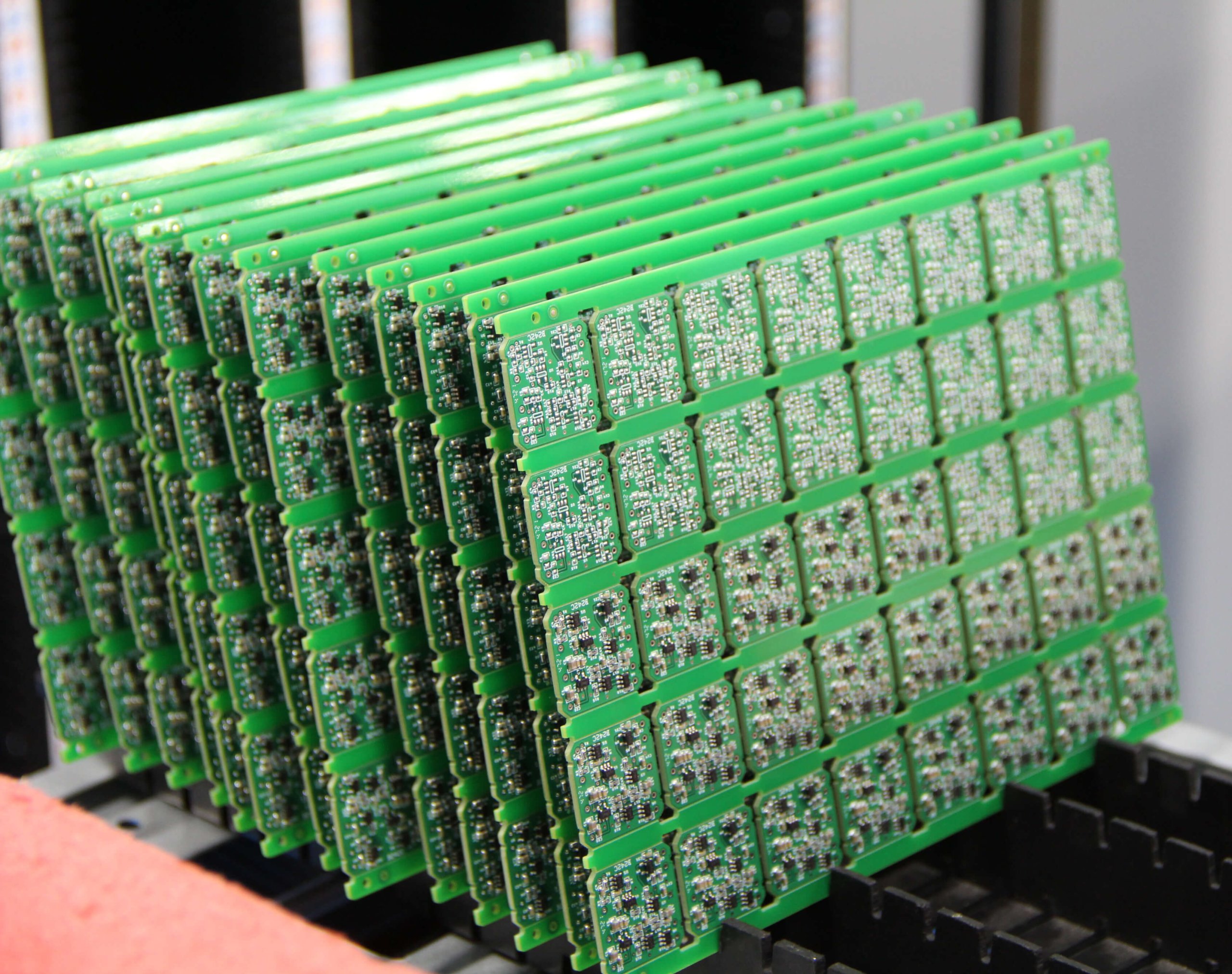
Keep Best PCB Assembly Co., Ltd is a printed circuit board assembly manufacturer integrating component procurement/SMT/DIP/finished product assembly and testing.
Our Value
Three core advantages help customers succeed in business
- Participate in R&D proposals and reduce the number of R&D samples, from initial samples to trial production to mass production.
- The trend of customization and personalization is obvious, orders are scattered, small, and fast.
- Understand customers’ quality thinking and be familiar with international communication methods
Our repair and return policy
The first PCBA manufacturer in the industry to provide the ultimate in high-quality services.
Can be returned or exchanged
No physical objects, no photos, no reason to return or exchange, as long as you are satisfied.
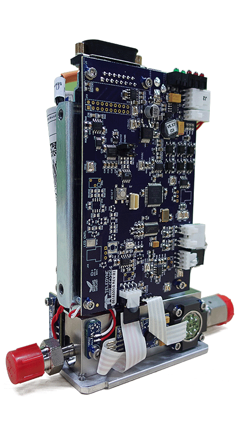
If you want to have it repaired locally,
We bear the cost of repairs
If you agree to return it for repair,
We cover logistics and repair costs
If you do not agree to repair,
We will replace you with a brand new product
If you do not agree to repair and replacement,
We will refund you
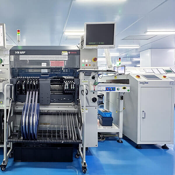
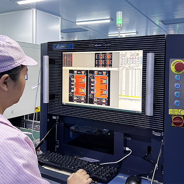
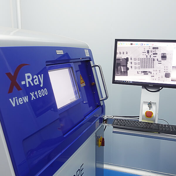
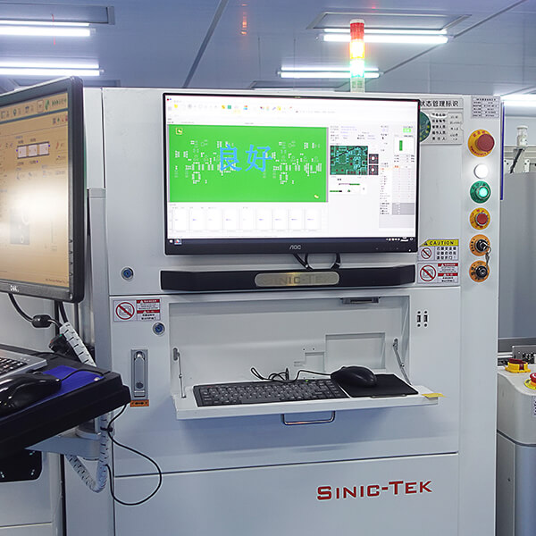
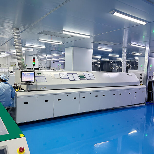
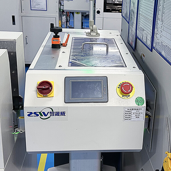
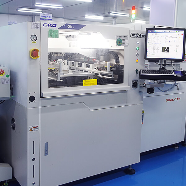
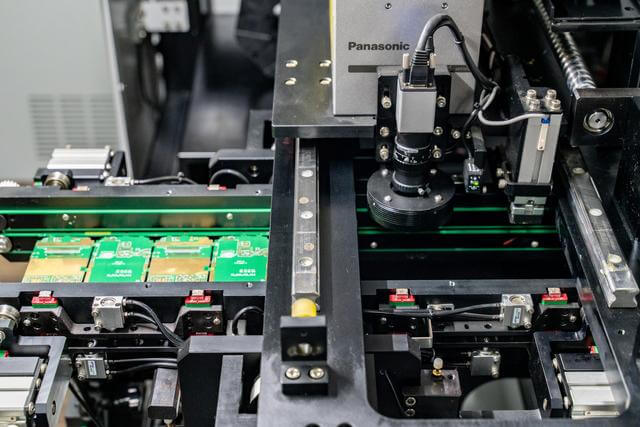
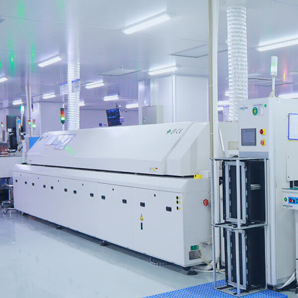
Machinery and equipment
Our production equipment
Our advantage
Why us?
1
Extreme quality control
There are 19 processes for quality inspection, and each process follows the strictest standards in the industry.

2
Mature
team
A professional team with an industry average of more than 12 years of work experience.

3
Precision equipment
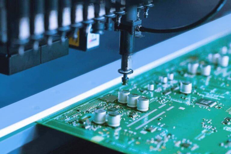
Use advanced equipment with high precision, high speed and high reliability for production and testing.

4
Efficient system
Digital intelligent ERP and MES systems improve high-efficiency production and high informatization level.

5
supply chain management
Formulate 14 guidelines for regular evaluation and assessment from various aspects such as product quality and sustainability.

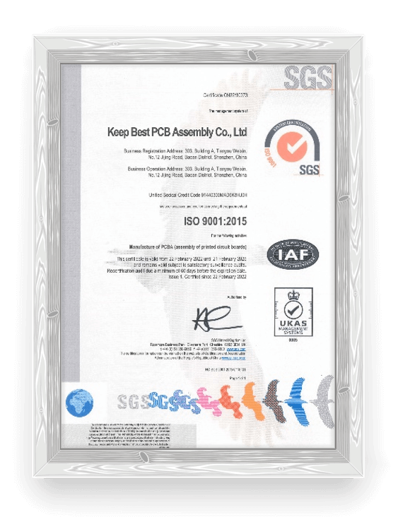
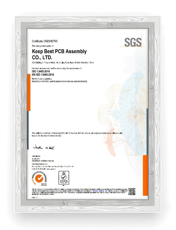
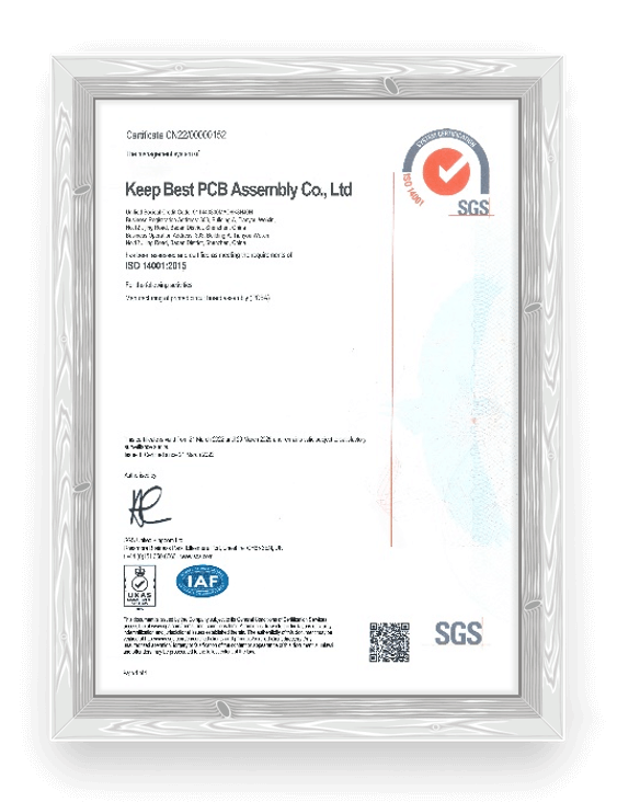
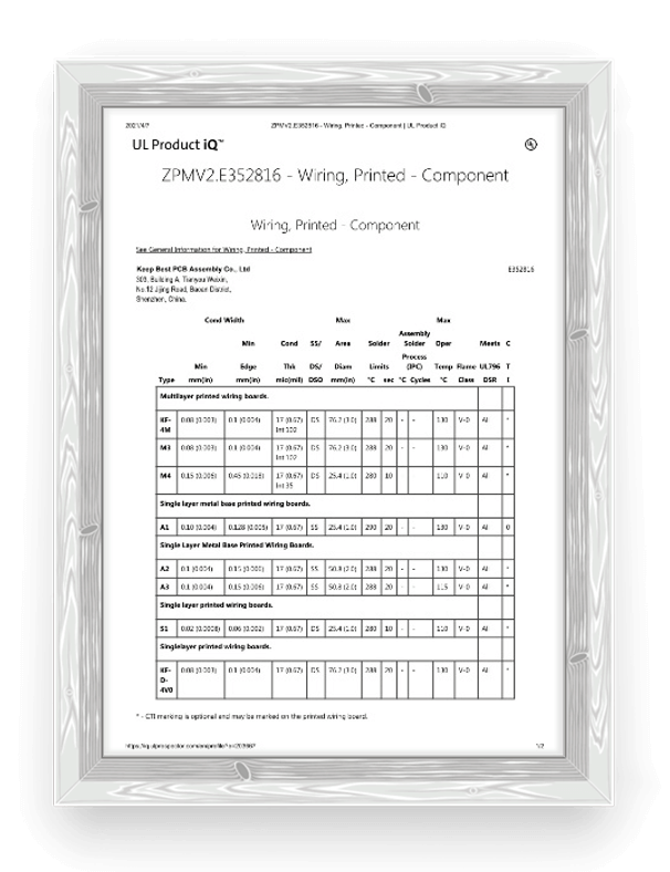
We have obtained multiple international and domestic quality certifications and strictly follow international standards.
What do others say
Customer testimonials
Take a look at what our previous customers have to say about us and make the right choice for your purchase.
I am very satisfied as a customer of Keepbest Company. Their PCBA products are of excellent quality, with prompt delivery and considerate service, making them a trustworthy partner.

Keep Best has been our trusted PCB and PCBA supplier for over five years. Their products are of exceptional quality, and their customer service is impeccable. We highly recommend them to anyone looking for a reliable and experienced PCB manufacturer.

Keep Best is our go-to PCB and PCBA manufacturer. Their products are top-notch, and their prices are very competitive. We have never had any issues with their products or services, and we are always confident that we can rely on them to deliver high-quality products on time and within budget.
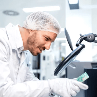
After years of cooperation with Keep Best, we have been deeply impressed by their professional PCB assembly expertise and consistent quality standards. Their products have consistently maintained zero defects (verified by AOI/X-ray inspection), and we are extremely satisfied with their performance.

Our Case
Industries we serve
We have many years of experience in the PCBA industry, which allows us to deeply understand our customers’ needs and provide the most suitable solutions and the highest quality services for them.
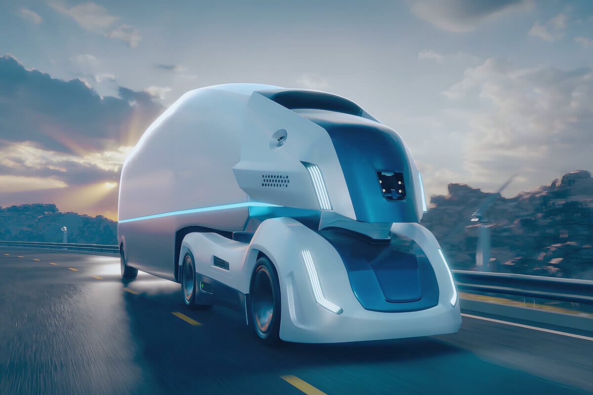
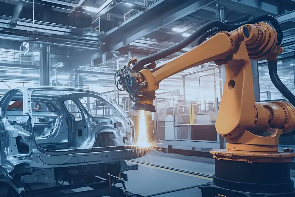
Automobile
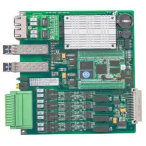
PCB Assembly
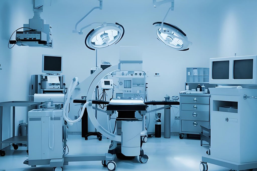
Medical
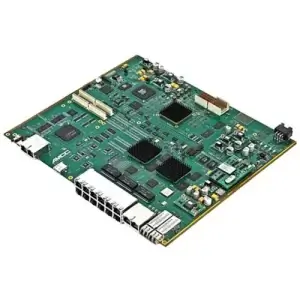
PCB Assembly
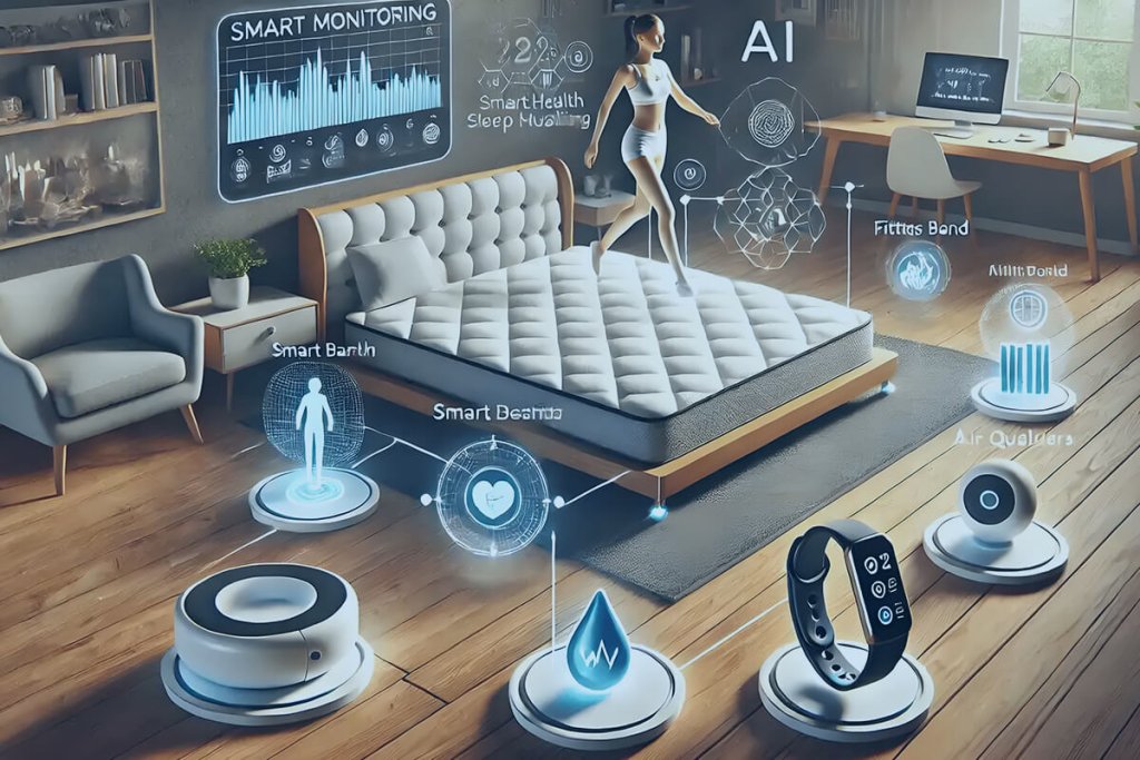
Industrial Control
PCB Assembly
Internet of Things
PCB Assembly

Internet of Things
PCB Assembly
- Phone:+1 (859) 254-6589
- Email:info@example.com

artificial intelligence
PCB Assembly

artificial intelligence
PCB Assembly
- Phone:+1 (859) 254-6589
- Email:info@example.com
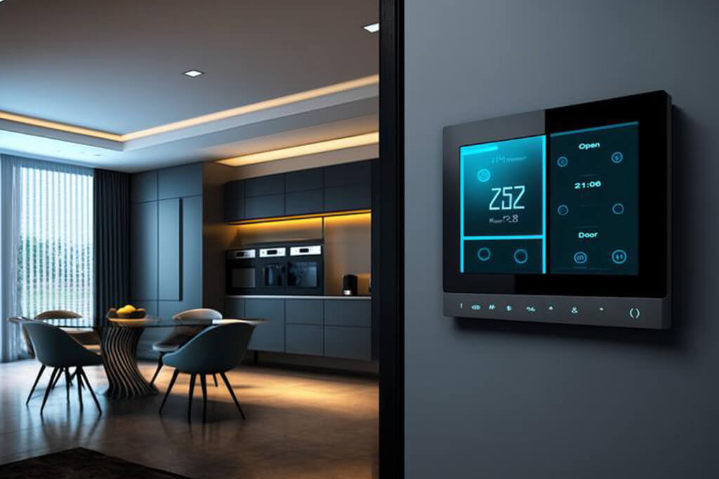
smart home
PCB Assembly

smart home
PCB Assembly
- Phone:+1 (859) 254-6589
- Email:info@example.com
FAQ
We mainly focus on high-quality PCBA services of "multi-variety, small and medium batches, and short delivery time"
Usually under 100 pieces are classified as low-volume PCB assembly services, which requires a reliable PCB assembler to meet these needs.
Low-volume PCBA assembly can provide high turnaround times without leaving PCBA boards stuck in high unusable inventory.
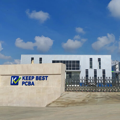
Yes, we are fully capable of providing PCB manufacturing and PCB assembly capabilities. We have a factory of 50,000 square meters. You can contact us if you need it.
Our estimated delivery times start the day after you place your order, depending on the volume and complexity of your turnkey PCB assembly requirements.
A complete turnkey PCB assembly service offers multiple benefits including ease of management, low or high volume assembly, multiple services, fast lead times, and more!
Offering turnkey PCB assembly services means that the supplier will handle all tasks including component or part sourcing, manufacturing, assembly and final delivery!
Yes, we can provide both services at the same time.
Yes, you can count on us for mass production of lead-free PCB assemblies.
For sure, we have advanced facilities and equipment to handle a large number of PCB orders. In addition, we have a team of PCB experts with extensive experience in meeting high volume PCB production.
Choose Keepbest and have no worries!
To satisfy our customers is our constant aim.
We are committed to making our products zero-defect and can return or exchange them for you without any reason.

