


Have you ever wondered how your smartphone can be so powerful and still go right into hand? Currently, there is an increased demand for more powerful yet smaller devices. The problem, however, is that traditional printed circuit boards (PCBs) cannot perform well because of their limited potential in terms of component density and miniaturization.
This is where High-Density Interconnect (HDI) PCB design steps in. This new technology addresses these limitations of traditional PCBs by finer features and high-density interconnect in nature. HDI boards use advanced concepts, including tiny micro vias, blind and buried vias, and extremely thin traces.
This enables to packing of multiple components in smaller spaces. Want to know more? This article provides all aspects of HDI PCB design, its advantages, types, challenges, and applications.
Let’s get started!
Key Advantages Of Using HDI PCBs
HDI PCBs are perfect for modern electronic devices because they offer several important advantages. Let’s discuss these benefits.
- Reduced Board Size and Weight:Since they are smaller and weigh less, HDI PCBs are ideal for use in compact and lightweight devices, with mobile devices being a good example. Advanced techniques, such as the above-mentioned microvias and blind/buried vias or thin traces, allow for more components within a smaller area. It also makes the devices more portable and convenient to use.
- Increased Functionality:With HDI PCBs, designers can fit more components within smaller areas, resulting in increasingly feature-rich devices. That’s allowed hardware manufacturers to adjust high-resolution cameras, faster processors, and more sensors in smartphones and tablets. Hence, there’s no reason to make the PCB any larger.
- Improved Performance:HDI PCBs enhance the performance of electronic devices by reducing signal path lengths. This results in improved signal integrity and faster transmission speeds. It also decreases the possibility of signal loss and interference. Thus providing better performance and reliability for devices like routers and switches.
- Potential Cost Savings: Due to cutting-edge manufacturing technology, HDI PCBs cost more in initial design and fabrication. However, they can also save costs in the long run. Smaller sizes and fewer parts mean fewer material costs and shipping expenses. Furthermore, fewer boards are needed due to increased functionality, which cuts costs.
Types And Structures Of HDI PCBs
Now that we have explored the many advantages of HDI PCBs, it is important to know which types and structures enable these benefits. There are several types of HDI PCBS, and they offer different advantages based on their construction and the type of vias used. Let’s have a look at each of them!
- Build-up HDI:These are multi-layer circuit boards that use microvias to transfer the electrical connections from one layer to another. Tiny holes also interconnect the layers, known as Microvias. These enable more high-density components and finer routing. Therefore, build-up HDI PCBs are ideal for very dense and compact applications.
- HDI with Buried Vias: These HDI PCB vias are hidden inside the board’s core material. Since buried vias connect only the inner layers, more components can thus be placed on surface layers. This structure is very useful if we work on a design that needs more internal connections without crowding external layers.
- Sequential Build-up HDI: These HDIs also combine buried vias and blind vias to form complex interconnect structures. Blind vias connect the outer layers to the inner ones without passing through the board entirely. This method is perfect for more complex designs that have to route many options and need a high level of interconnect density.
Challenges And Considerations In HDI Design
After discussing different types of HDI PCBs, discussing the problems while designing them is essential. While HDI PCBs provide several advantages, they also come with certain complications. So, let’s jump into some of the key factors that designers should consider:
1.Stricter Design Rules:
HDI PCB components are smaller and the tolerances are tighter, so great design and layout practices must be followed. Such mistakes can be easily avoided during place and route of the components.
These stringent requirements can be met with the help of advanced design software which also runs on rules-driven engine as mentioned. Remember: When it comes to HDI designs, little mistakes are negligible.
2.Advanced Manufacturing Processes
Special equipment and expertise are needed to manufacture HDI PCBs. More advanced techniques must be used, such as laser drilling for microvias and sequential lamination.
They are significantly more precise and refined than traditional methods. However, advanced manufacturing can also increase cost and lead time. Therefore, it is very important to work with an experienced manufacturer who has insight into these processes and can achieve quality output.
3.Signal Integrity Concerns
Keeping signal integrity right is challenging as more components are packed into smaller spaces. A high-density layout can create problems such as crosstalk or signal loss, negatively affecting high-frequency application performance.
Designers must use tools that provide simulation capabilities of electromagnetic interference (EMI) and signal response. Such tools help identify predictable problems early, enabling necessary adjustments. Proper planning and full simulation are important for minimizing signal integrity problems and ensuring your HDI PCB will operate reliably and efficiently.
4.Thermal Management
Due to their high component density, HDI PCBs produce a lot of heat. Good thermal management is very important because if the device overheats, it will damage components and reduce lifespan.
Designers should follow strategies to deal with the heat. Such as thermal vias are small, conductive holes of heat that help to transfer the hot spots to other places and thus ensure even distribution. Metal heat absorbs and dissipates heat efficiently.
In addition, using high-thermal-conductivity materials and thermal pads to conduct heat from components into the PCB reduces heating. Good PCB layout planning ensures that any heat-generating component is always adequately spaced.
Applications Of HDI PCBs

However, besides the benefits achieved, these challenges make HDI PCBs extremely valuable in various applications. HDI PCBs are used in many applications. They offer compact size, improved performance, and greater functionality. Let’s explore some common areas where HDI PCBs excel:
1.Smartphones and Other Mobile Devices
HDI PCBs are a great helper for smartphones and tablets. The devices must comprise small, light, but high-performance components.
The technology enables manufacturers to integrate features such as high-resolution cameras, powerful processors, and memory into shrinking form factors. As you can see, the superior connectivity offered by HDI PCB allows modern mobile devices to accommodate extremely complex functions.
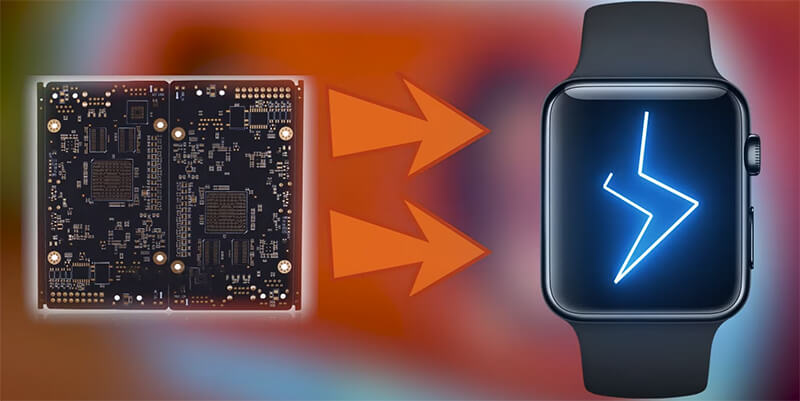
2.Wearable Electronics
Wrist-worn wearables such as smartwatches and fitness trackers use HDI PCB to have a smaller footprint with advanced features. At the same time, they need to be lightweight, durable and power-efficient.
HDI PCBs help achieve this miniaturization, allowing these wearables to integrate sensors, processors, and communication modules into a tiny package. It improves the user experience by offering them cutting-edge functionality without adding bulk to their smartphone.
3.High-Speed Communication Devices
HDI PCBs are used to handle intricate circuitry in a small area, such as routers, switches, and other high-speed communication devices. HDI technology significantly enhances signal integrity and transmission speed, which is critical in high-frequency data exchange.
This guarantees the former real-time and fast communication necessary to achieve an optimal level of performance. HDI PCBs reduce signal loss and crosstalk, so the data rate and quality remain good.
Robust construction is required to ensure that the HDI PCBs are durable and reliable. This will allow them to function continuously in various environments. It lowers downtime and maintenance costs, allowing your system to keep performing at peak levels continually.
4.Medical Electronics
Medical Electronics, such as implantable devices and imaging equipment, require accurate functioning and reliable reliability. HDI PCBs are also very useful for much more complicated and advanced medical applications, which can benefit from their miniaturization and high density.
HDI PCBs are also crucial since they allow for the functionality and durability critical when dealing with healthcare applications. Such as implantable devices that need to be very small while still being extraordinarily reliable. HDI PCBs are designed to withstand these functions, offering the flexibility and performance these life-saving technologies need.
5.Automotive Electronics
In the automotive sector, these PCBAs are used in advanced driver assistance systems (ADAS), infotainment, and other electronic control systems. HDI PCBs are used due to their strong performance and small size in these applications.
It can withstand harsh car conditions, such as temperature fluctuations and vibrations. What’s important, however, is that it is dependable and contributes to making modern vehicles better and safer. Car manufacturers are able to make their electronic systems durable and efficient, which in turn makes our cars smarter and safer.
Conclusion
Overall, the HDI PCB design represents a significant step forward in electronic design and production. HDI technology provides a way to produce more powerful yet reliable smaller products by providing higher layered utilization than conventional PCBs.
Nowadays, HDI PCBs play an important role in smartphones, wearable electronics, high-speed communication devices, medical equipment, and other technological products. With so many benefits and applications, HDI PCBs are bound to be an integral part of the future of electronics.