


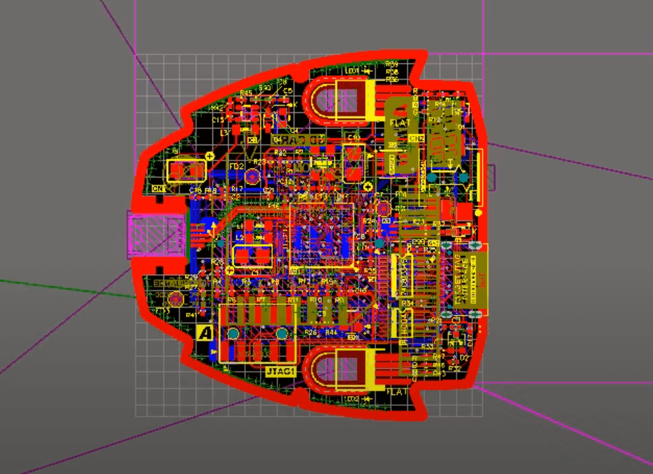
PCB design creates layouts interconnecting electronic components on a board using multiple design layers. The conductive layer handles electrical connections, while the mechanical layers provide physical details like the board’s dimensions, the locations of holes, and how the components should be assembled.
But what are these mechanical layers, and why are they essential in PCB design? Don’t worry; we’ve got your back. This article will examine the different mechanical layer types, their benefits, and important design concerns. So, let’s get started!
Types of Mechanical Layers in PCB Design Software
Mechanical layers are non-conductive layers in the PCB design software. It helps to provide critical physical information about the board. Here are its main types:
- Board Shape: This layer defines the overall outline or contour of the board. Its purpose is to define the board’s accurate dimensions and shape, ensuring that it fits perfectly within its enclosure. This layer also acts as the cutter’s guide during PCB cutting.
- Board Edge Cuts: This layer defines the location and size of any slots, cutouts, or chamfers along the borders of the PCB. Such parameters are necessary to create more complex board contours or specific component requirements, such as connectors and mounting slots.
- Holes:This layer describes the size, location, and type of all the holes on the PCB. Holes can include plated through-holes, which fulfill electrical connections between layers, and mounting holes that allow the PCB to be secured. An exact overview of the holes is required for effective component mounting and electrical connections.
- Silkscreen: This layer offers a non-conductive visual layer for markings like component reference designators, logos, and assembly instructions. It helps identify components and mark where each part needs to go on the board, and it can contain other important information, such as polarity indications or test points.
Assembly Notes (Optional): This is one more optional layer that provides extra details for the PCB assembler, such as where to put components, how to solder, or anything related to assembly notes. All the details above will help ensure the correct and efficient assembly of the PCBs.
Advantages of Using Mechanical Layers in PCB Design
Now that you know the types, it’s time to jump into the benefits of mechanical layers, which guarantees that the final product is reliable and manufacturable. Here’s how they help:
- Improved Design Communication: They visualize physical dimensions and component placements for fabrication partners. This transparent communication guarantees that all parties engaged in the manufacturing process understand the design requirements and helps to minimize misunderstandings.
- Enhanced Manufacturability:Mechanical layers reduce the chances of a future issue during fabrication. They make sure that the design complies with the limitations of the process involved and is easy to produce, resulting in less time consumption.
- Error Prevention: They provide the engineer with a visual representation of component clearances and overall board dimensions. This reduces errors and ensures that everything fits together without interference or overlap.
- Streamlined Assembly: The silkscreen layer helps provide proper component placement and clear assembly instructions. Assemblers then find it easy to place solder components accurately in the desired position, achieving high efficiency and increasing overall accuracy in assembly.
Creating and Managing Mechanical Layers
Since mechanical layers have many benefits, as you are aware, PCB design requires careful planning and execution, which involves a few key steps to ensure accuracy and completeness:
1.Defining Design Rules
Before you begin routing, create design rules for every mechanical layer. This includes dimensioning parameters like hole size, minimum clearances, and silkscreen text sizes. These rules help maintain consistency and avoid any unwanted issues while designing from one end to the manufacturing on the other.
2.Populating the Layers
Use proper design tools within your PCB design software. Each mechanical layer needs to be populated with relevant information.
For example, you’ll specify the board shape, place holes, and silkscreen markings. Remember to check that all the details, such as physical dimensions, cutouts, and hole locations, are indicated correctly.
3.Verification and Review
Finally, before sending the design to production, verifying the mechanical layers for accuracy and completeness is vital. This can be done with 3D views of the board and examination of fabrication drawings.
Check that the design has proper spaces, alignments, and overall integrity. Such a review might help eliminate issues before they become critical and ensure that the design meets the specifications.
Conclusion
Mechanical layers in PCB design contribute to the much-needed support structures and information that make the final product manufacturable, reliable, and effective. The more you can learn to use and properly program the mechanical layers, the better prepared your PCB design will be for manufacturing success.