


The design of interdigitated electrodes in PCBs can be complicated, especially when high sensitivity and accuracy are required from the sensors. So, if you also find it exceptionally difficult to learn how to design interdigitated electrodes in PCB, do not worry; help is here to work for you.
This article is intended to take you step by step through the process of design, giving you tools and confidence to make effective interdigitated electrodes for your PCBs.
Therefore, let’s get started.
What are Interdigitated Electrodes in PCB
Before getting straight to how to design interdigitated electrodes in PCB, it’s essential to first understand what exactly they are.
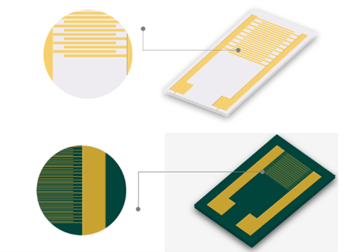
Well, PCB interdigitated electrode structures are components used in various sensors and electronic devices. They are mostly fabricated from two interleaved or interdigitated comb-like arrays of electrodes, which look like the fingers from two neighboring hands put together.
This increases the sensitivity of the sensors by a major extent, as does their surface area.
But, what are the applications and working principles of sensors according to IDEs? Let’s discuss this in detailed below.
Applications and Working Principles of IDE-based Sensors
Here are some common applications and working principles of IDE based PCBs:
- Capacitive Sensors
Capacitive sensors measure the changes of capacitance developed between interdigitated electrodes. With an external factor, for instance, be humidity or touch affecting the dielectric between the interdigitated electrodes, this will result in a change in capacitance.
The resultant change can be measured and further used in sensing the external factor. Typical uses include touch sensors and humidity sensors.
- Resistive Sensors
Resistive sensors utilize the differences that exist in resistances seen between interdigitated electrodes. Any substance, including gas and liquid, that comes into contact with this surface alters the resistance on it. A gas sensor and gauges used for strains depend on it.
- Bioimpedance Sensors
Bioimpedance sensors were intended to measure impedance, which in reality is the opposition to AC current existing between the interdigitated electrodes. In most of such sensors, it is medical diagnostics or wearable health monitors to measure such properties as body composition and hydration levels.
Now that you understand what interdigitated electrodes are in PCB, let’s see how we can design them.
Key Design Considerations for IDEs on PCBs
Making interdigital electrodes on a PCB almost always involves serious considerations to achieve better functional performances with reliability.
These are some of the major points to take into account during design.
1.Geometric Parameters
The geometry is a very important parameter as the performance of an IDE is greatly affected by it. Length and width of fingers are important parameters, because longer fingers make the interaction area larger, making the IDE more sensitive; however, this could also increase noise.
Wider fingers enhance current-carrying capacity but seriously reduce the resolution critical for accurate measurements.
Another important parameter is the spacing between the fingers, or pitch. Smaller spacing provides a better sensitivity, since more interactions take place between electrodes; however, it can make the microfabrication process more complicated, maybe requiring more precise manufacturing techniques.
Consistent and accurate spacing within the device is highly essential in actual sensor performances to be correct, ensuring that capacitance, resistance, or impedance changes can also be accurately detected in a reliable manner.
2.Material Selection
Material selection is one of the most important aspects in the performance of an effective IDE. One must also take proper care to select the right conductive material. Copper is a commonly used material, since it does well electrically and, as a result, it is cost-effective.
It adheres to well to PCB substrates, but it may require further protection from being oxidized. Whereas gold costs much more, it guarantees better conductivity, as well as resistance to oxidation. Silver is also preferred due to its outstanding conduction capacity compared to gold, but it could tarnish, which would affect performance in the long term.
Besides this, other considerations include reliability for good adhesion to the PCB substrate and ease of manufacturability—factors that are important with fine-pitch or complex designs. The choice of material should adhere to the PCB substrate for long-term reliability.
3.Dielectric Layer
The dielectric layer is of particular importance in capacitive sensors since it acts as a medium between the electrodes and significantly affects their capacitance. In fact, the sensitivity of these sensors is determined by the material’s dielectric constant. Normal conditions indicate that higher dielectric constants will increase the sensitivity, in the sense that the sensor can detect lower changes in the environment.
The dielectric layer can also be made of a variety of material options. Polymers are flexible, easy to apply, but they might have a touch on the sensitivity with reduced dielectric constants. High dielectric constants are offered by ceramics, and so do higher stability values, though they could be a bit hard to integrate into the PCB design.
The right dielectric material will be chosen because it will impact how fast the sensor shall be in responding to the situation and how sensitive it is to give accuracy and precision toward the changes within the environment.
These geometric parameters, material selection, and the role of the dielectric layer can maneuver in a way to design efficient interdigital electrodes for PCBs meeting the performance and reliability standards.
Now, let’s go through the design process for IDEs on the PCBs.
Design Process for IDEs on PCBs
These are the steps through which you could design interdigitated electrodies in PCBs:
Step #1: Defining the Application of the Sensors
The very initial design process will require a clear definition of what the sensor application is. This means one has to know what the sensor is being aimed at and its performance requirements.
Determine the sensitivity range, the type of changes the sensor needs to detect (e.g., capacitance, resistance, impedance), and the operating frequency.
With these parameters set early enough, the guidelines will inform every decision you will make along the way into the design process so that the product will be fit for its intended use.
Step #2: PCB Design Software
Using the right PCB design software is crucial for creating accurate and efficient IDE layouts. Some of the modern PCB design tools come along with a number of features that can make the process of making a design much more efficient:
- Trace routing tools: All these tools enable the placement and routing of electrode traces in the correct manner, allowing a geometrically correct layout with regard to finger length, Spacing, and finger width.
- Design rule checkers: These are the features that design rules conform to the possibilities of manufacturing so that layouts are possible and within the tolerances of a PCB manufacturer.
The features of rule check in both routing and trace design will save a lot of time and reduce errors during the design stage.
Step #3: Layout Techniques
Creation of the IDE layout involves the application of defined geometric parameters to a design. Make sure that the spacing between the interdigitated fingers in the layout is kept correctly to show the desired sensitivity and performance.
Important factors include:
- Finger Length and Width: These are to utilize the stage results as it is a geometric parameter. Make sure fingers are sized with the right size, subjected to a sensitivity and noise balance.
- Spacing and Pitch: To maximize uniform sensor performance, the spacing between sensing elements has to be minimized, while maintaining the least possible variation in this spacing across the sensor, therefore also facilitating a simple manufacturing process.
Proper care in the use of layout techniques ensures IDEs, when implemented, will function correctly and effectively.
Step #4: Simulation
Prior to simulation, one can utilize the simulator tools to predict the performance of the IDEs; simulation will provide some insight into the behavior of the design under several conditions and reveal issues that might not have been apparent during layout.
Some more benefits of a simulation are as follows:
- Performance Analysis: Determine how performance will be affected by changes in capacitance, resistance, or impedance.
- Optimization: Modify design parameters and optimize them on simulation results with the aim to improve sensitivity, accuracy, and performance in general.
It is an optional step that adds value, but the risk of design flaws in the final product is reduced.
Challenges You Might Face When Designing IDEs on PCBs
Here are design hurdles commonly faced by people while doing IDEs on PCBs:
Fabrication Accuracy
Ensuring that such accuracy in fabrication is reached is essential to assure that the designed trace widths and spacing are kept. Work closely with your PCB manufacturer to make sure they can meet the required tolerances. High-precision techniques for fabrication will be imperative so as to get the desired performance from the sensor.
Consider the following:
- Precision Fabrication: Choose an assembly facility with a reputation for a high percentage of precise PCBs.
- Quality Control: Conduct good, detailed quality control to meet fabrication specifications designed for the PCBs.
Material Compatibility
Check the compatibility of materials used with the chosen conductive material and PCB substrate. In addition, correct adhesion is essential to reliability and good performance in the long term.
Consider these tips:
- Material Properties: Make sure the conductive materials are compatible with the substrate—compatibility in terms of adhesion and thermal expansion.
- Environmental stability:Ensure the materials can resist environmental conditions to which the sensor would be exposed, which could include temperature changes and humidity.
Signal Integrity
Signal integrity for high-frequency sensor applications has to be maintained by considering grounding and shielding techniques that reduce interference and signal losses.
Key considerations are
- Grounding: The necessary ways of grounding needed in order to prevent noise in the signal.
- Shielding: Use shielding to protect the sensor from electromagnetic interference (EMI).
Conclusion
So through following a structured design process and solving key challenges, you have ensured effective and reliable interdigitated electrodes for PCBs are realized.
That way, it remains ensured that the applications are designed adequately regarding the fabrication accuracy, compatibility of materials, and integrity of signals with the needed performance standards of the IDEs.