


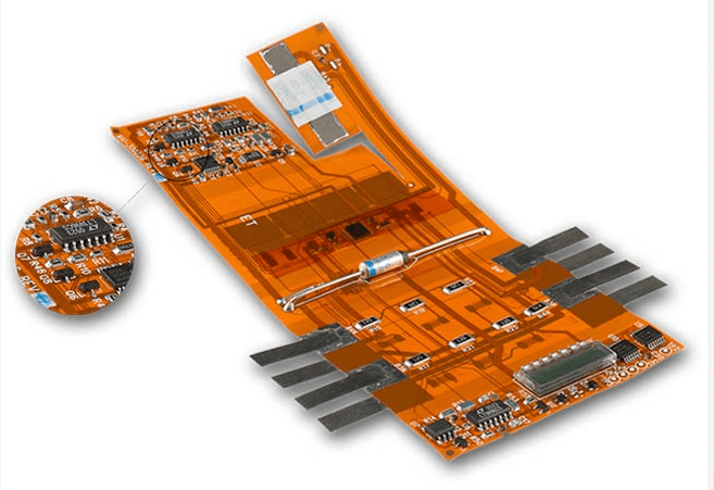
A single-layer flex PCB or a single-sided flex PCB is a type of PCB that only features electronic circuits on one side of the flexible substrate. Even though this PCB first appeared on the market in the 1950s, it remains well-liked today, and there are multiple reasons for this. The most significant advantage of its continued popularity is the diverse application area.
The structure of a single-layer flex PCB is the following: the flexible substrate (usually polyimide) serves as a basis for a bending copper layer that conducts the current. Afterwards, one or two protective layers cover this layer, protecting the printed circuit from external factors.
The article’s analysis will cover the following points: the definition of a single-sided flex PCB, its structure, main advantages and fields of use, the step-by-step approach to designing and developing technologies, the difficulties and their overcoming, and the manufacturing and reliability conditions.
Advantages Of Single Layer Flex PCBs
The evolution of technology is the reason behind the increased need for electronic components that are effective, small, and adaptable. Below are some of the benefits of this circuit and the preferred choice in the current design of electronic circuits.
1. Flexibility
Thanks to their capacity to bend, twist, and conform to various shapes, flexible circuits are ideal for use in tight spaces that require frequent adjustments. While rigid PCBs are confined to plane patterns, flexible circuits can form in three dimensions. These are the aspects of current electronics that fuel small and versatile devices.
2. Weight Savings
Flex PCBs are ideal for wearable and portable devices where every gram counts because they are composed of far lighter materials than rigid ones. Thus, smartphones and smartwatches frequently use flex circuit boards to lighten weight and improve comfort.
3. Design Freedom
Flexible PCBs open up new horizons for the design of small and highly efficient electronic systems. Engineers are empowered to create innovative device configurations, a feat that was once impossible with rigid PCBs. The ability to accommodate multiple features on a single flexible PCB, without the need for connected rigid boards, saves significant space in small devices, sparking a wave of creativity in the electronics industry.
Applications Of Single Layer Flex PCBs
The demand for adaptable and small electronic components is rising as technology develops. Because of their unique qualities, single-layer flex PCBs are vital in many sectors. Let’s examine their main uses and how they affect contemporary electronic gadgets.
1. Wearable Electronics
Flexible PCBs, with their superior flexibility and lightweight nature, are not just a technological marvel, but also a practical solution for portable devices like fitness and health monitors. Their use enhances the overall comfort of these devices, which are often worn on different body parts. The ability to withstand physical strain further enhances their reliability and durability. Moreover, the reduced weight of the flex circuit board contributes to the overall lightness of the device, making it easier to carry for extended periods.
2. Keyboards
Flex PCBs are also notably popular in the keyboard industry for producing responsive and durable interfaces. The flexible design allows users to create ergonomics with an improved user experience. In addition to regular computer keyboards, single-layer flex PCBs are used on membrane switches and flexible keypads for the end equipment of consumers, industrial controls, and medical equipment. The flexibility of circuits allows for the development of lightweight, thin, yet reliable input devices.
3. Medical Devices
Flex PCBs are crucial in medical devices as they can bend, shape, and flex to the human body’s requirements and anatomical constraints. Commonly found in devices such as hearing aids and pulse generators, PCBs offer biocompatibility using biologically safe materials like polyimide and copper foil.
Moreover, their flexible and rigid nature helps manufacturers produce small devices, especially wearable and implantable devices. This eventually leads to small and functional devices coupled with stability and reliability for patients.
Designing A Single Layer Flex PCB
There are a few essential steps in the design process to ensure a single-layer flex PCB satisfies all specifications. Let’s examine the key steps in designing a dependable, efficient, flexible printed circuit board.
1. Defining Design Requirements
The design process should start by defining the design requirements. It is essential to consider whether the flexible PCB is required to be flexible, including the flexibility, bend radius, and environmental factors. This is important so the flexible PCB will work as expected in the application.
The bend radius must be calculated so there is no cable fracture risk. To ensure the durability of flexible circuit boards, it is essential to take into account environmental conditions such as temperature and humidity.
2. Material Selection
Choosing the right materials is crucial for the effective performance of a flex PCB. The required properties are flexibility, electrical characteristics, and successful workability. Substrate materials, such as copper and protective layers, are usually produced based on polyimide or polyester.
Both polyimide and polyester have superior flexibility and robustness properties. Polyimide withstands high temperatures and mechanical pressure, making it suitable for high-performance applications. The copper layer should be flexible but thick enough to ensure good current-gripping properties.
3. Schematic Capture
The schematic comes afterwards. This graphic illustrates internal electrical connections. At this stage, it is important to be guided by design requirements to depict the schematic as close as possible to the future layout of the actual circuit.
This picture can be correctly gathered from schematic details using the design software, and the result, so to speak, will be a guideline for PCB layout. Furthermore, the picture above shows that such an image must also demonstrate all components, their connections, and everything special to a flexible circuit.
4. PCB Layout
The schematic should keep all parts about how they are translated to a PCB layout. The engineer should use design software to reroute the imaged photo procedures; the engineer will also place parts to help the flex circuit remain flexible and straight while keeping an eye on maintaining vaults, pinwheels, and signals.
Imaged photo processes are the most common way to identify circuit patterns in imaged processes. It is possible to keep parts away from flex-circuit placements, particularly in high-risk areas. The engineer anchors the parts in place to prevent any movement.
5. Routing
Unfortunately, routing traces on a flexible substrate is not as simple. The user is not allowed to stress the traces for the long-term reliability of the PCB. There is the correct routing—avoiding sharp bends, adapting, and improving transitions as much as possible.
Moreover, impedance should be controlled, especially for high-speed signal lines. Additionally, routing design rules should be established regarding the mechanical properties of the flexible PCB; the traces are specifically positioned to cause as little material strain as possible.
6. Design for Manufacturing (DFM)
Design for manufacturing, or more colloquially, DFM, is the most critical. It involves the minimum bend radius, the locations of the vias, and assembly constraints. DFM is required to ensure a flex PCB’s manufacturability and reliability.
Vias must be positioned to avoid high-stress zones, and the designer must rework the design to fit within the process limitations. In addition, any landmark areas must be cushioned with stiffeners composed of FR4 or steel.
Specific Challenges In Single-Layer Flex PCB Design
Engineers must overcome difficulties when designing a single-layer flex PCB to guarantee performance and dependability. They must comprehend these difficulties and find solutions to build flexible circuits of the highest calibre.
- Flexibility and Bend Radius: Engineers must consider the minimum bend radius limitations to prevent damage during bending and operations. Design rules guarantee that the flex PCB keeps its integrity under stress. Tighter bend radii necessitate extra-strong materials and routing to avoid stress fractures in the copper layer.
- Stress and Fatigue: Maintaining long-term functionality requires stress and fatigue management. Cracks and failure are possible with repeated bending and mechanical stress. Staggered trace routing and ensuring traces are at right angles to the bend can help the engineer and high-wear material substrates such as polyimide and premium copper foil.
- Material Compatibility: The material should be compatible with the substrate, copper layer, and components. Appropriate materials commonly lead to various manufacturing and operational difficulties and quality dissipation. Meanwhile, the adhesive chosen for bonding the copper foil with the substrate layer must also be compatible with both layers. The photo-imaged processes guarantee accurate layer alignment and bonding, preserving the flexible circuit’s build integrity.
Manufacturing Considerations: Flex PCBs have unique manufacturing challenges. Routing accuracy and components placed in the right place on the flexible substrates would demand an array of precision. How these Flex PCBs were made, laser cutting or high variability on a precision drill also required the designer to cooperate with manufacturers and follow their instruction guides to attain the quality for producing Flex PCBs.
Conclusion
Ultimately, designing a single-layered flex PCB is difficult and overwhelming. There are multiple stages, all of which are complicated to approach if the designer needs to understand the available materials, possible layouts, or manufacturing opportunities.
However, the design guidelines are properly followed, and the knowledge of the advantages and disadvantages of flexible circuits is preserved. In that case, creating an entirely novel and reliable solution for thousands of different electronic devices, from wearables to the most advanced medical equipment, is possible. Similarly, with proper planning and preparation on the manufacturer’s part, it is feasible to realise the benefits of flex PCBs.