


PCB antennas are already integral to most traditional and current digital devices in the sector due to factors like integration ability, low consumption, and wide range. Thus, they are becoming more mainstream and can be found in many vehicles and intelligent clothing.
It becomes a cost-effective method to cover diverse ranges by framing electromagnetic waves from electric demand to each recipient or object. They represent a viable and sustainable solution to minimising the number of physical documents and the high-performance cost for many technologies. This paper discussed PCB antennas’ qualities while presenting their advantages, potential usage, form factors, and pattern.
Advantages of PCB Antennas
Due to its many advantages, PCB antennas are becoming a common option for contemporary electrical gadgets. The main benefits are as follows:
- Small Size: These include small-size PCB antennas ideal for devices with limited space. They can easily be integrated into smaller devices and lightweight products such as smartphones, wearables, and IoT gadgets. This makes it easier for manufacturers to produce smaller and portable devices.
- Low Cost:PCB antennas are affordable since they are made from cheap materials like copper and are produced efficiently. Since they are integrated into the PCB, they do not require extra components and less material is used during production.
- Ease of Integration: PCB antennas can easily integrate into existing PCB layouts without needing connectors or external components, simplifying the design process. Such integration reduces assembly time and the number of potential points of failure, thus improving device reliability.
- Design flexibility: PCB antennas demonstrate flexibility in design as providers offer extensive design options. Engineers can optimize antenna designsby varying their shape, size, placement, frequency, and radiation pattern, thus applying them to perform multiple tasks.
Applications Of PCB Antennas
PCB antennas’ adaptability, small size, and dependable performance make them essential for various applications. Here are a few typical and crucial uses:
1. Smartphones
PCB antennas are also used for various other reasons the phone was manufactured. They support the ability of people to make phone calls via cell systems. In addition to data connections using 2G, 3G, 4G, and 5G networks through a phone or gadget, one can achieve fast data connections via the phone’s Wi-Fi. A high-speed system also supports the ability of people to surf the web.
People can stream music videos and other uploads over the Internet. The phone’s Bluetooth PCB uses Bluetooth to connect it with accessories such as headphones. Phones also have GPS, which enables the user to determine directions.
2. Wireless Routers
PCB antennas are critical in creating strong Wi-Fi connections in wireless routers. They ensure that several computers, smartphones, tablets, and smart home appliances are always connected and working perfectly without any connectivity issues. PCB antennas also help maximize the signal strength and distance covered and eliminate “dead areas,” ensuring that Wi-Fi is always available in a bigger area.
3. Wearable Devices
Their small size has made PCB antennas increasingly popular in wearable technologies. For example, they are used in fitness trackers to communicate with a user’s smartphone to sync data and provide real-time updates. Similarly, they are included in smartwatches to enable notifications, calls, messaging, and Internet searching.
Moreover, health monitoring devices are borrowed to wirelessly send health data to mobile applications and the physician or healthcare system. This offers convenience and flexibility, so even infectious conditions can be efficiently monitored remotely.
Types Of Pcb Antennas
PCB antennas come in various forms, each with special qualities and uses. The main categories are as follows:
1. Monopole Antennas
Monopole antennas have one radiating element mounted perpendicular to the ground plane. They are well-known for their simple design and omnidirectional signal reproduction. Because they send an equivalent signal in all directions, they are ideal for use outside structures that want a consistent signal distribution.
Monopole antennas are used in cell phones, wireless communication gadgets, and specific IoT devices. Their simplicity allows for their simple configuration within PCB layouts, achieving good results that can be deployed in many wireless devices.
2. Patch Antennas:
Patch antennas, or micro-strip antennas, consist of a flat rectangular or circular copper patch over a grounding plane. Owing to their compact size and simple structure, they are most suited for microwave frequencies and are highly demanded in portable devices.
They are also commonly employed in GPS, satellite communication, and RFID systems. They have instant high gain and may be directional; thus, this antenna is best suited for applications necessitating a limited signal transmission. Depending on the frequency of the antenna, the patch might have varied geometric figures.
3. Fractal Antennas:
Fractal antennas are designed using intricate geometric shapes, typically repeating shapes, to enable multi-band characteristics and a reduced size. These types of antennas can operate efficiently at various distinct frequencies, which is an essential feature in devices that require the use of multiple bands.
Some examples of such devices include smartphones, complex communication systems, and other gadgets. They are also advantageous because they use minimal space. The complex shapes support a compact size, yet the antennas work just as well. As such, antennas are necessary when space is an issue, and the devices must operate across varied frequencies.
PCB Antenna Design Process
A PCB antenna’s design must take into account several important factors to guarantee top performance and dependability:
1. Antenna Requirements:
The first design step is to define the antenna requirements. The most critical parameters in this regard are:
- Operating Frequency:This involves selecting the frequency within which one intends to deploy the antenna. This is essential in making the antenna compatible with the system for which it has been designed.
- Bandwidth: Bandwidth describes the range of frequencies an antenna can effectively cover. A higher bandwidth indicates that the antenna performs well across a larger frequency range.
- Gainrefers to an antenna’s ability to effectively direct energy in a specific direction. A high gain strengthens the signal and extends its coverage distance.
Radiation Pattern: It is to provide the radiation pattern that outlines the spatial distribution of the radiated energy. This is crucial as it explains how the antenna radiates in different areas.
2. Antenna Selection:
After defining the requirements and design constraints, the appropriate antenna type should be selected based on the following factors:
- Size:The antenna size should fall within the project’s design constraints.
- Cost: The cost of the materials and manufacturing process should work within the budget.
- Performance: The chosen antenna’s performance should meet the project’s requirements for gain, bandwidth, and radiation pattern. Common antenna types includemonopoles, patch antennas, and fractal antennas.
3. PCB Layout:
Integrating the antenna into the PCB layout is critical to ensure proper performance and signal integrity. Some of the aspects to consider include:
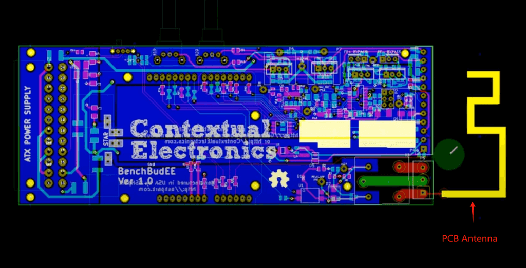
- Component Placement: Place the antenna where it is least interfered with while optimising its performance. Position it at the corner of the PCB for maximum clearance since this location also provides the best radiation pattern.
- Ground Plane Design:The antenna requires a properly designed ground plane. A good ground plane design guarantees signal integrity and minimises electromagnetic interference.
- Routing:Ensure routing of traces that do not result in signal loss and guarantee proper signal integrity. Maintain short traces, straight when possible, and ensure proper impedance matching.
4. Simulation and Optimization
The simulation process starts with creating the extensive antenna model and the PCB layout, which is finalised by importing it into simulation software after being set with those parameters. In the following step, the above parameters are simulated, and a dozen simulations are run to predict the antenna’s performance and get the gain, radiation pattern, and impedance. This allows the designer to fix some of the design errors and create an antenna that should work properly in real space without interference.
5. Testing and Validation
Testing and validating the antenna’s performance is the final process to verify whether the antenna meets the required specifications. The correct measurement techniques and tools, such as vector network analyzers and anechoic chambers, are used to obtain the needed data.
Thus, validation is realized to identify if the antenna exhibits the required gain, radiation pattern, and efficiency. Furthermore, the measured results are also compared with the predicted ones by simulation; discrepancies are also noted. Depending on the test results, necessary modifications are made to the design, and the validation process is redone until the best optimal results are acquired.
Common Challenges and Considerations in PCB Antenna Design
If developing a PCB antenna is under consideration and is to operate optimally and reliably, severe challenges and concerns need to be addressed.
1. Antenna Performance
Antenna performance is the biggest challenge to take measure and demands satisfying specific gain, radiation pattern, and efficiency. Gain indicates the antenna’s capacity to concentrate energy in a particular direction. The radiation pattern defines its coverage area, while efficiency measures how well the antenna converts input power into radiated energy.
2. Signal Integrity
Signal integrity between the antenna and the transceiver circuitry should be high quality. Signal integrity helps prevent signal loss and degradation. Some signal integrity factors include trace routing, impedance matching, and shielding. Good trace widths and lengths, as well as reduced bends and vias, promote signal integrity.
3. Electromagnetic Interference (EMI):
EMI should be reduced to prevent unwanted disturbances. It originates from the PCB components and external sources, causing noise and signal loss. However, proper grounding, shielding, and component placement may help manage EMI. Spacing, ferrite beads, and filtering methods should also reduce EMI.
Conclusion
Ultimately, PCB antennas require proper design since numerous nuances harm their performance. To sum up, every aspect of the advantages, applications, and types, as well as the design procedure itself, the correct installation procedure, signal integrity, EMI reduction, and simulation software, must be paid attention to. All this diligent attitude to the most minor details combined with a wise approach can make the devices work better, providing more stable and secure connections within a short period.