


Looking to learn how does the 2 layer PCB design work? Well, many engineers and PCB designers struggle when it comes to understanding 2 layer PCB designs.
But don’t worry, in this article, we are going to discuss 2 layer PCB design process step by step. This will help you understand what is 2 layer PCB design, its pros & cons, its applications, and how the designing works.
So let’s get started.
What is 2 Layer PCB Design
Before getting straight to how does 2 layer PCB design work, it’s essential to first understand what is it.
Two-layer PCB design refers to a two-layered circuit board design in which two layers of conductive material are separated by a non-conductive substrate material. Normally, a two-layer PCB is made of fiberglass epoxy.
These layers connect electronic signals from the integrated circuit through resistors, capacitors, connectors, and through-hole devices.
In a 2-layer PCB design, one layer of the conductive material would generally be used to route traces, while another layer would be reserved for the ground plane or power plane to offer a fixed-voltage reference or ground reference for components.
Structure and Components of 2 Layer PCB Design
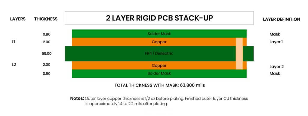
This is the basic 2-layer PCB stack-up:
- Substrate Material: FR-4 fiberglass epoxy is typically used as the support.
- Copper Foil Layers: Two layers of conductive laminate attached to the substrate.
- Component Placement: Assembled components on the PCB surface for interconnect.
- Traces:Thin conductive pathways connecting the components.
- Vias: Small holes are drilled through the substrate to connect layers.
- Solder Mask:An insulating layer that ensures there is no possibility of a solder bridge.
- Silkscreen: Ink layer with all component designations and any other graphic support.
Pros and Cons:
|
Pros
|
Cons
|
|---|---|
Applications of 2 Layer PCB Design
Below are some of the usual applications where 2-layer PCB designs usually used:
- Consumer Electronics: Simple devices range from calculators, remote controls, and digital clocks.
- Sensor Interfaces: Devices equipped with sensors for the environment.
- Circuits Consuming Low Power:Devices using batteries, for instance, wireless peripherals.
- Control Systems: Simple household, industrial, or automotive controls.
- Interest: Kits for learning electronics and hobbyist projects.
- IoT Devices: Basic smart switches and home automation gadgets.
- Industrial Controls:Relay Boards and Low-Power Motor Controllers.
Now you know the basics of 2 layer PCB design, it’s time to learn how does it work.
How Does 2 Layer PCB Design Work
This is how the PCB designers come up with 2-layer PCB design:
Step #1. Schematic Capture:
First, the engineers will sketch an image of the circuit using the schematic capture software. They decide which symbols are for the components and which lines to use to connect them.
Step #2. Design PCB Layouts
They then drag the blocks of the circuit diagram onto a virtual board and arrange them so that they look nice and the signals flow gracefully from one to the next.
Step #3. Routing:
They draw lines on the board to connect the components. The lines carry electrical signals. They need to be careful so that the lines do not touch each other.
Step #4. Design for Manufacturing (DFM):
Design for manufacturing assures that a PCB can be built without any problem. Engineers have to think about how to choose the right materials, stick to the rules and standards, and make things easy to put together.
That way, they will be able to point out errors in advance of manufacturing, where.
So that’s how 2 layer PCB designing work.
Common Challenges and Considerations in 2 Layer PCB Design
During the design process, there are some common challenges you might face.
So here they are:
- Limited Routing Space:
The routing of the complicated circuits in 2-layer PCBs might be tough, as there would not be enough space left for trace routing between parts of components.
The engineer would then have to plan very carefully how the signal would be kept apart, and this would interleave other routing between parts of components.
- Signal Integrity:
Keeping signals clear and strong is super important. In 2-layer PCBs, signals may mix up with each other or easily pick up noise.
Things like trace length, proper alignment, and separation of signals from anything that could mess them up are of great concern to the engineer.
- Regulated Impedance:
Making sure that signals travel at the right speed can be very difficult on 2-layer PCBs, especially for fast signals or things like Wi-Fi.
For this reason, engineers must be very careful with regard to how wide the traces are, how far apart they are, and what materials they are made of, in order to ensure that the signal is strong and constant.
- Power Distribution:
The key is getting power to all parts of the PCB properly. If power isn’t distributed right, parts might not get enough juice, or they might get too much noise.
They need to make sure power goes where it is supposed to and that it is clean and steady. They also use some special parts to help keep things stable.
Conclusion
In conclusion, understanding 2-layer PCB design is essential for engineers and enthusiasts alike.
With careful planning and attention to detail, 2-layer PCBs can be successfully designed and manufactured, paving the way for innovative electronic devices to come to life.