


Do you find it difficult to ensure smooth production and meet specifications with your PCB designs? Understanding the meaning and importance of DFM in PCB design is the key to scaling through such hurdles.
Do not worry; you are not lost. In this guide, we will discuss everything about the DFM concept and take you through how it can potentially transform your PCB design process.
So, let’s just start.
What is DFM in PCB designing?
DFM (Design for Manufacturing) in PCB design is a set of guidelines that aims at designing PCBs that are effective in terms of cost and are produced effectively.
This selection and optimization of the layout of the PCB include the processes for design for fabrication (DFF) and design for assembly (DFA).
As DFM considers the manufacture standards and constraints of PCBs at a design stage, the need for redesigns is thus reduced, the time to market is reduced, and overall product quality increases.
Some of the common DFM guidelines followed in PCB designing include:
- Sufficient spacing should be maintained between the components to allow for proper soldering.
- Keep the thickness of the board uniform for structural uniformity.
- Use regular sizes of the components so that it does not get overcomplicated during the assembly process.
- To reduce complexity and chances of errors in assembly, reduce the number of unique parts.
- Keep in view the thermal and electrical loads on the printed circuit board to ensure reliable operating conditions.
So, these guidelines help to craft a PCB that is not only functional but manufacturable, cost-effective, and reliable.
Efficient Production and Fulfillment of the Specifications
DFM in PCB design, as described earlier, is more of a process that ensures production efficiency, providing boards based on the requirements.
The DFM, if followed by the designing process, would anticipate and prevent potential issues in the manufacturing process, such as the parts that are not easy to solder or PCBs that would need much manual work.
This will smooth the production process proactively and ensure that, with consistency, quality levels are kept in final products for greater reliability and customer satisfaction.
Besides, DFM is one principal part of the PCB development life cycle, serving as a channel of connection between the design and manufacturing.
Now that you know the basics of DFM in PCB design, it is time to touch on the benefits.
Advantages of Incorporating DFM Principles in PCB Designing
There are multiple advantages of incorporating DFM principles in PCB designing. Some of the most important ones are:
- Reduced Costs:By optimizing designs for manufacturability, DFM helps identify and eliminate potential manufacturing inefficiencies, ultimately reducing production costs.
- Improved Manufacturability: DFM ensures that PCBs can be produced more efficiently, with fewer errors and less rework required during the manufacturing process.
- Higher Quality: By addressing manufacturability issues early in the design phase, DFM helps enhance the overall quality and reliability of the final product.
- Faster Time-to-Market: Streamlining the manufacturing process through DFM principles can accelerate product development cycles, allowing for quicker time-to-market for new PCB designs.
Key Factors to Consider During PCB Design for Manufacturability
When it comes to PCB design for manufacturability, several key factors play a crucial role in ensuring smooth production and high-quality results. Some of them are:
- Component Selection:Choosing components that are readily available and compatible with the manufacturing process is crucial for smooth production and cost-effective assembly.
- Footprint Design: Properly sizing and positioning component footprints on the PCB layout is essential to prevent assembly errors and ensure optimal performance during manufacturing.
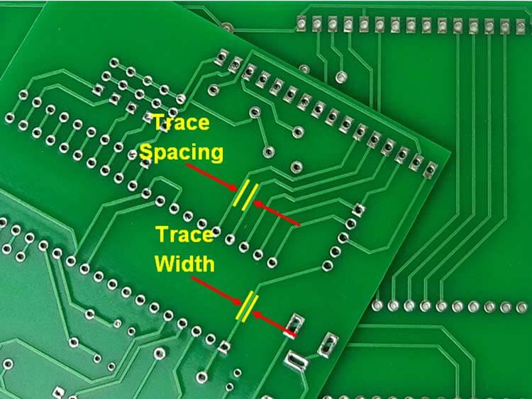
- Minimum Feature Sizes: Adhering to minimum feature sizes for traces, pads, and vias helps maintain manufacturability and prevent issues such as short circuits or open circuits.
- Solder Mask Application: Ensuring proper application of solder mask is vital for protecting exposed copper traces and preventing solder bridges during assembly.
DFM Challenges in PCB Designing
By following the guidelines of DFM in PCB designing, there are some common challenges you might face.
- Thin Trace Widths:Designing traces with widths that are too narrow can lead to difficulties during manufacturing and may compromise signal integrity.
- Tight Clearances: Inadequate spacing between components or traces can result in solder bridges or electrical shorts during assembly, impacting the functionality of the PCB.
- Complex Via Structures: Overly complex via structures can increase production costs and pose challenges during the manufacturing process, particularly with regard to drilling and plating processes.
- Solderability Concerns: Issues with solderability, such as poor wetting or inadequate adhesion, can lead to soldering defects and reliability issues, affecting the overall performance of the PCB.
By being aware of these common challenges and implementing strategies to address them early in the design phase, designers can mitigate potential risks and ensure the successful production of high-quality PCBs.
Conclusion
In conclusion, incorporating DFM principles into PCB design is essential for achieving efficient production processes, reducing costs, and ensuring high-quality end products.
By addressing potential manufacturing challenges early in the design phase and optimizing the design for manufacturability, designers can streamline the production process and enhance overall product reliability.